
Projects & Initiatives
How and where does ficonTEC contribute to the integrated photonics eco-system development scene?
As part of the on-going development of our technology base, and also as part of our contribution into the development of the sector, ficonTEC is pleased to have previously been, and be currently actively involved and associated with numerous national and international projects and initiatives.
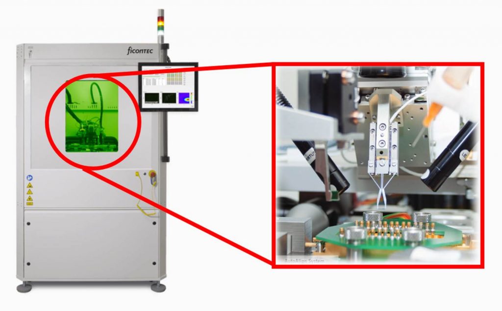
For the activities and interactions listed below – and so too for any developments necessary for specific customer requirements – ficonTEC relies on its dedicated R&D Center, located close to ficonTEC HQ. Manned by highly qualified, mostly Ph.D.-level (over 70%), but also highly experienced personnel, the team is central to ficonTEC’s regular and respected contributions to the assembly and testing development scene. The R&D Center is equipped with a variety of specialized assembly machines, a 3D printing system, die testing machines, wire bonders, cross-section capabilities, a die shear tester, etc., and has achieved several significant milestones in photonics micro-assembly.
Want to know more about ficonTEC’s assorted project involvements?
Contact us
PolyChrome
Photonic integration platform for sensory and analytical applications in a wide wavelength range
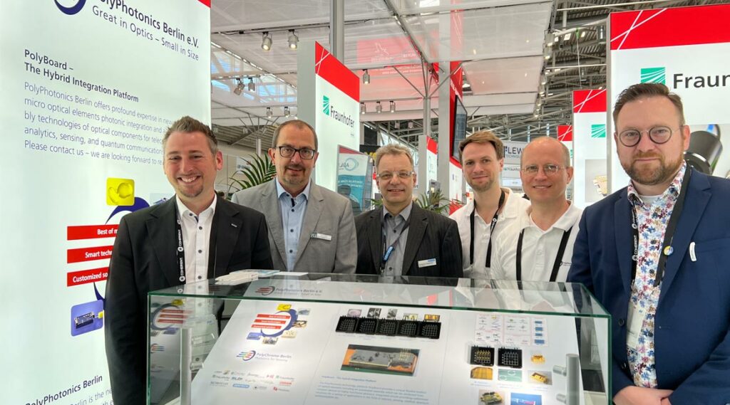
The PolyChrome Berlin alliance started in September 2022 with an expected duration of three years. The alliance consists of nine industrial partners and three research partners, including Fraunhofer Institute for Telecommunications (Heinrich-Hertz-Institute, HHI) which is leading the alliance. See the PolyChrome website for a list of partners. According to its research topics, the alliance is divided into five joint projects. These projects cover the basic materials technologies, functional components and construction technologies, as well as the assembly technologies for a total of six demonstrators for three different fields of application (fiber sensors, laser sources, SiN sensors). The aim is to develop a wide range of applications of microsensors not only in the near infrared, but also in the visible wavelength range.
ficonTEC is responsible for tailoring the handling tools to the specific needs of the components as well as, together with Fraunhofer HHI, for the development and qualification of the optics assembly process, leading to a new automated PolyBoard sensor production platform. Particular attention is paid to the flexibility of the system, so that it is possible to switch between series production of different demonstrators without much effort. A video of the assembly process for the Correlation Rapid Precision Sensing (C-RPS) demonstrator can be seen below, the assemblies of the other demonstrators will follow as the project progresses. ficonTEC leads the design of the SiN sensor demonstrators where different approaches for the implementation of a cost-effective mass-producible disposable are evaluated. An optical interface to the evaluation device and the design of the PIC are also developed. In a later step, the disposable and the optical interface are assembled using a specially developed ficonTEC system.
The PolyChrome Berlin alliance was preceded by the PolyPhotonics association, which developed HHI’s own polymer based PolyBoard technology and studied its assembly. The assembly of the optical elements on the PolyBoard is done using a ficonTEC CL1500 system.
Funded with a total amount of €13 million by the German Federal Ministry of Education and Research (BMBF), PolyChrome Berlin is part of the program line Regional Business Alliances for Innovation (RUBIN). RUBIN is intended to initiate processes in structurally weak regions that will lead to a competitive profile of the region in the long term. This creates regional value chains and innovative products.
PolyChrome Photonic integration platform
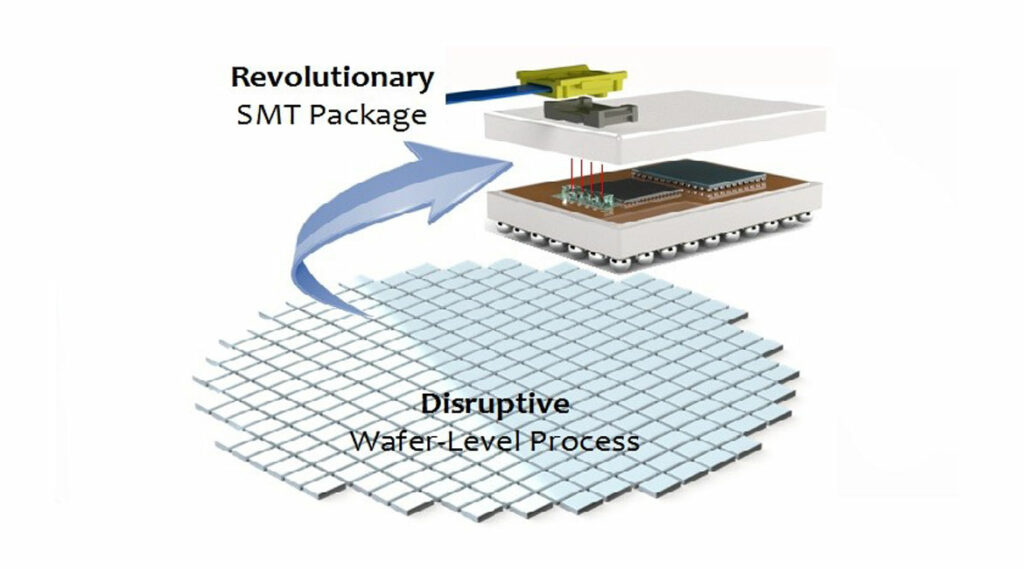
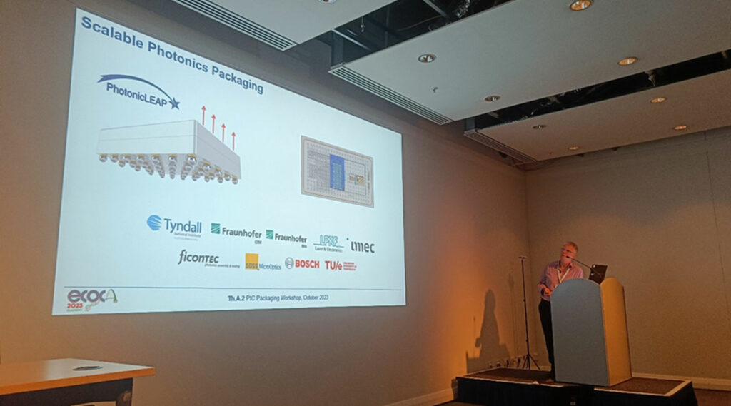
PhotonicLEAP
Disruptive low-cost photonic packaging and test technologies
PhotonicLEAP will develop disruptive wafer-level PIC module integration, packaging and test technologies that are designed to reduce the costs of PIC production by more than a factor of 10, thus promoting a new global standard for cost-effective PIC devices and high-throughput PIC testing, and in turn revolutionising existing applications and creating completely new markets.
PhotonicLEAP will use these disruptive technologies to produce a revolutionary surface mount technology (SMT) PIC package, which for the first time incorporates multiple optical and electrical connections and that can be scaled from low to very large volumes.
The project will validate these technologies through two state-of-the-art demonstrators, including a high-speed optical communication module and a portable medical device for cardio-vascular diagnostics. Furthermore, the technologies will be transferred to the flagship European PIC Packaging Pilot Line, PIXAPP, for future commercialisation. PIXAPP has an extensive and growing user-base across multiple global markets.
PhotonicLEAP is a European H2020 collaborative research project and is due to run until the end of 2024.
Update December 2023
The Photonic LEAP project and its goals were demonstrated at various events and exhibitions in 2023. Among these were demonstrations at Photonics West, PIC International and Laser World of Photonics Munich.
In addition, the article “PhotonicLEAP project awarded €5 million in EU funding”, highlighting the development of impactful photonic packaging and test technologies was published by optics.org.
At the ECOC in Glasgow, a presentation on laser soldering of Si PICs to glass substrates was held by Kevin Shortiss, titled “New Process and Equipment Development”. Peter O’Brien demonstrated the project as part of a workshop hosted by Tyndall and AIM Photonics
Peter O’Brien from Tyndall National Institute
Optik-Net
Direct flexprint technology for cost-effective integration of optical waveguides and electronics
Within the OptiK-Net project, an interdisciplinary team of industrial and research organizations will establish a process chain for the world’s first industrial solution for cost-efficient and flexible optical networks based on PCBs and printed polymer waveguides. An optical communication interface with high data rate is to be built as a first demonstrator.
ficonTEC’s role within the project is, amongst others, to develop a new assembly process using a 6-axis robot to handle, passively align and optically and mechanically connect the flexible polymer waveguides to the optical board, while minimizing assembly times and maximizing throughput.
OptiK-Net is a BMBF-funded project within the funding initiative ‘Miniaturisierte optische Systeme hoher Integrationsdichte’ (‘Miniaturized optical systems with high integration density’) and is due to run from October 2019 until September 2022.
Also interesting: R&D – OptiK-Net to develop direct flexprint technology…read more
CALADAN
Reducing manufacturing cost of Terabit/s-capable optical transceivers
The CALADAN project brings together a supply chain that will enable automatic wafer-scale assembly of Terabit/s-capable optical engines through the use of the Micro-Transfer Printing (mTP) technology. SiGe BiCMOS drivers and receivers and GaAs quantum dot lasers will be integrated onto silicon photonic integrated circuits, fully at the wafer level.
Coordinated by IDLab, an imec research group at the Ghent University, the ultimate goal is the fabrication of optical transceivers at significantly lower cost and higher throughput than what is achievable using current fabrication methods. This requirement is driven by the growing capacity of data center servers, and so too the links between those servers.
ficonTEC role within CALADAN will be to demonstrate automated fast ‘through-substrate’ fiber-alignment and bonding capability. A key aspect is to show that via the development of a fast fiber attachment process, how the optical packaging-costs and cycle-times can be reduced in a manufacture environment. ficonTEC already has a very fast handling and assembly process for optical fibers that allows fiber align-&-attach with sub-micron accuracy.
CALADAN is an initiative of the Photonics Public Private Partnership (PPP) and has received funding from the European Union’s H2020 innovation programme. It is due to run from January 2019 until December 2022.
TERIPHIC
Moving on to Terabit transceiver modules, and how to assemble them
TERIPHIC’s goal is to go beyond current 400G transceiver module standards and push development to Terabit transceiver modules having at least 2km reach. To achieve this, TERIPHIC will leverage photonic integration concepts and develop a seamless chain of component fabrication, assembly automation and module characterization processes as the basis for high-volume production lines.
ficonTEC will contribute by optimizing assembly processes and hardware on a ficonTEC CL1500 system already in use at the Fraunhofer HHI, thus supporting the development of the required automated assembly hardware appropriate for high-volume manufacturing for as yet to be detailed module-specific align-&-attach processes. In the final stages of the project, ficonTEC will put forward a concept for the entire high-volume production line.
Ultimately, the new transceiver design introduced by TERIPHIC will allow significant cost savings, not only due to assembly automation at the TOSA/ROSA stage, but also at the packaging level, and resulting in a cost below 1€/Gbps for the transceiver modules.
So far, ficonTEC has developed a highly elaborate gripping tool for emitter and detector arrays. When these arrays are gripped, the outermost devices can still be probed and operated to allow for fast and precise active alignment. The arrays are then aligned and attached to a polyboard arrayed waveguide grating as part of the transmitter and receiver optical subassemblies (TOSA/ROSA) of the Terabit optical transceivers being developed within the TERIPHIC project. Novel alignment concepts are being investigated to allow for a precise yet fast alignment and attachment of the components, which then will be part of a high-volume production line concept for the Terabit optical transceivers.
The gripping tool as well as the alignment concepts currently being evaluated can later be transferred to comparable processes, where component arrays (e.g. arrays of emitters, detectors, fibers, lenses, etc.) must be aligned actively, thus enabling new markets to be explored.
TERIPHIC is an EU H2020 project starting January 2019 and due to run for 36 months. More details can be found at Fraunhofer HHI and via the EC’s CORDIS website.
Article – TERIPHIC consortium goals in the News
The Horizon 2020 funded consortium TERIPHIC is developing new optical transceiver modules used in Internet datacenters that will reduce power consumption by 50% per GB/s and in turn see lower carbon emissions…read more

By loading the video, you agree to YouTube's privacy policy.
Learn more
TERIPHIC ICT project
MASSTART (completed)
Mass manufacturing of transceivers for the Terabit/s era
The inherent issue of limited throughput and the associated high cost in photonics assembly and test processes is unsurprisingly a major hurdle to the introduction of new photonic developments into the consumer market, and one that can only be solved by cost-efficient assembly solutions. The MASSTART project will tackle exactly this problem with a well-chosen consortium dedicated to the development of a high-throughput assembly line for transceivers for the Terabit/s era. Briefly:
- MASSTART aims to provide a holistic transformation to the assembly and characterization of high-speed photonic transceivers, including a six-fold improvement in throughput. By bringing the cost down to €1/Gb/s or even lower in mass production, this will help guarantee European leadership in the photonics industry for the next decade.
- ficonTEC will develop concepts and assembly solutions for the automated mass production of photonic devices. A key aspect is the concatenation of different assembly stations into a single integrated production line with automated part handling. Orchestrating the whole via a higher-ranking process control will achieve the required high throughput.
- The first process demonstrations have been completed, and an initial machine concept comprising four passive adjustment stations has already been presented. In addition, new module plug types will be introduced to help provide more flexibility and reduce assembly overhead.
The developments performed within MASSTART will allow ficonTEC to maintain its technological leadership within the photonics assembly segment, provide better understanding of future industry demands, and thereby strengthen our position in the market – all while helping to guarantee European leadership within the global photonics industry.
MASSTART is an EU-funded H2020 project pursued by a consortium of renown European organizations and is due to run from January 2019 for 36 months.
Update December 2023
The MASSTART project came to completion in September 2023. For more information on the final review meeting at ficonTEC’s headquarter in Achim …
MASSTART update hereiQonic (completed)
iQonic project technology provider
Opto-electronic manufacturing is undergoing an evolution of the manufacturing and associated processes. This trend, together with the pressure to control production costs, imply that systems configurations need to change more frequently and more dynamically. In this scenario, automation and sustainability strategies are the most logical route to reduce the production costs. This alone lies right on our own product strategy path.
iQonic also aims to offer a scalable zero-defect manufacturing platform covering the overall process chain, ranging from the design of new opto-electronic components and their required optimized process chain, their assembly process, to their disassembly and reintroduction into the value chain at their end-of-life through eight scalable strategies.
ficonTEC is part of iQonic and is fulfilling the role of technology provider. The company has wide experience with photonics assembly and testing processes, and it is supporting the project in the design of a reconfigurable process chain and in the development of a new type of handling tool interface for opto-electronic assembly processes.
Update, November 2020: Sensap AG visits ficonTEC for the implementation of the data flow among the ficonTEC AL500 assembly machine. Read the news item here …
Update, November 2020:
The iQonic project came to completion at the end of 2022.
ficonTEC results within the iQonic project
Within the iQonic project ficonTEC developed the basic software tools for streaming data to and from Process Control Master, the general programming software for all ficonTEC machines.
In combination with the integration of industrial environmental monitoring sensors as additional data sources (to the sensors already present in the machines) and the setup of a data streaming network, all fundamentals have been established. The tools have been integrated into an Assemblyline A1200 machine from project partner Prima Electro running in full production mode. Using this set-up, successful data streaming was established, allowing the predictions from the project partners to be displayed in parallel to the ongoing assembly process and hence improving the overall yield of the machine.
ficonTEC A1200 assembly system for lens alignment, showing the process set-up inside
By loading the video, you agree to YouTube's privacy policy.
Learn more
By loading the video, you agree to Vimeo's privacy policy.
Learn more
JePPIX Pilot Line (supported by InPulse)
InP PIC manufacturing eco-system
Indium phosphide (InP) photonic integrated circuit (PICs) offer game-changing performance capabilities across multiple market sectors. The goal of the JePIXX Pilot Line is to put in place the technological and operational processes to accelerate the uptake of InP PIC technology in new markets, align scalable and interlocking services and value chains, accelerate time to market with predictive design for fewer and faster design cycles, and to offer foundry processes at TRL7, sharing process optimization across products.
Within the JePIXX Pilot Line project, ficonTEC will drive forward the acceleration and standardization of PIC device test procedures to high-throughput processes that are compatible across measurement domains.
By loading the video, you agree to YouTube's privacy policy.
Learn more
This will be accomplished using customizable, yet standardized scripting formats for testing and characterization in the optical and radio-frequency domains. Testing can be accelerated by utilizing state-of-the-art robotic handling and highly optimized optical alignment procedures.
The JePPIX Pilot Line is financially supported by the InPulse project, an EC-funded H2020 Manufacturing Pilot Line project for PICs utilizing indium phosphide, starting January 2019 and running for 48 months. Access to InPulse technology is via JePPIX, the Joint European Platform for Photonic Integrated Components and Circuits.
JePPIX Update Q1 2024:
Together with PITC (Photonic Integration Technology Center), ficonTEC and many more of our partners, we at JePPIX strive to make the test method a part of the PIC workflow (design for testing, DFx) thus paving the way to a testable design before committing to fabrication. Watch the video for more details. ‘
By loading the video, you agree to YouTube's privacy policy.
Learn more
AIM Photonics
A national PIC manufacturing infrastructure, widely accessible and inherently flexible
AIM Photonics (American Institute for Manufacturing Integrated Photonics) is an industry-driven public-private partnership that focuses the US’s premiere capabilities and expertise to capture critical global manufacturing leadership in photonics.
The Institute’s goal is to emulate the dramatic successes experienced by the electronics industry over the past 40 years and to transition key lessons, processes, and approaches to the photonic integrated circuit (PIC) industry. In doing so, AIM Photonics aims to support SMEs, providing practical access and technology on-ramps for US industry, government, and academic communities.
ficonTEC is closely following this initiative and ficonTEC US has already been selected among a list of suppliers. Our first contribution comes through the award of a contract for a new wafer-level automated tester, working in close cooperation with UoC (University of Columbia), SUNY (State University of New York), and RTI (Rochester Technical Institute).
By loading the video, you agree to YouTube's privacy policy.
Learn more
Tyndall National Pilot Line (completed)
An integrated photonics manufacturing eco-system at Tyndall National institute
Tyndall National Institute and ficonTEC Service have come together along with other industry partners to build the National Photonics Manufacturing Pilot Line, an integrated photonics manufacturing ecosystem designed to advance disruptive photonic technologies from concept to commercialization.
The Pilot Line, located within the Tyndall Institute (Cork/Ireland) will engage with sectors such as MedTech, Life Sciences and Communications. Tyndall is already the location of the PIXAPP Pilot Line Gateway (see below) and the Irish Photonics Integration Centre, which collectively provide access to leading-edge technology, highly skilled researchers and valuable infrastructure.
ficonTEC will establish a unique facility with a dedicated support team to develop advanced photonics manufacturing equipment for emerging markets. The Pilot Line will additionally train the future photonics workforce in advanced manufacturing processes, with particular focus on MedTech, a valuable sector not only in Ireland.
Funding is being provided by the Irish Government through its Disruptive Technology Innovation Fund (a €500m fund established under Project Ireland 2040), and is run by the Department of Business, Enterprise and Innovation, with administrative support from Enterprise Ireland. Access to the Pilot Line is open to any and all companies around the globe looking to quickly realize future integrated photonic devices within a dedicated ecosystem.
UPDATE: This project, funded by the Department of Business, Enterprise and Innovation has been completed successfully.
Primary outcomes of the project
There are three primary project outcomes. Firstly, the setup of a laboratory with automated assembly machines operating in conjunction with Tyndall’s packaging group. These can address R&D projects and develop processes and products for small volume production of optical packaging solutions. Secondly, the development of new assembly processes for more complex micro-optics and fiber array assemblies. And thirdly, the strengthening of academic and industry collaboration for photonics packaging in Ireland.
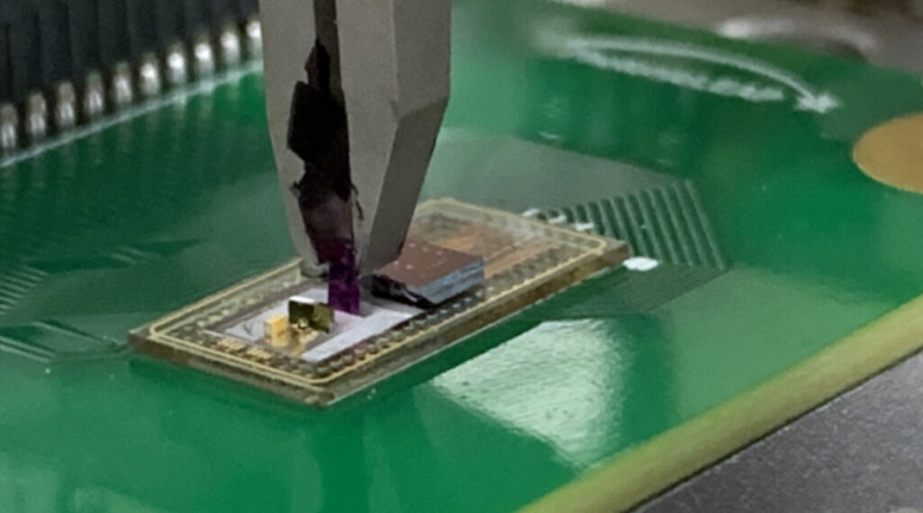
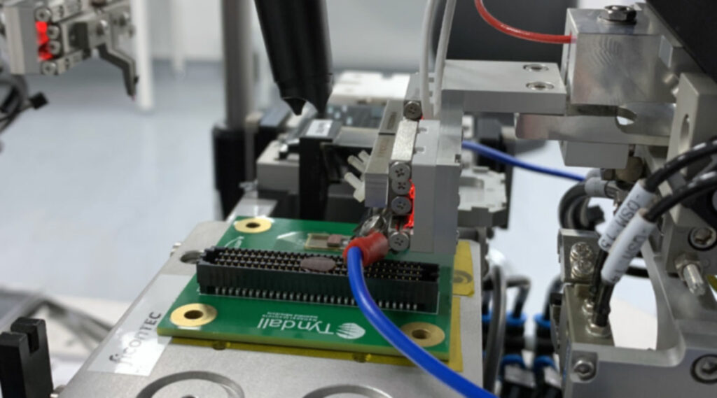
The alignment and assembly of a laser module with a collimating element and a refocusing lens to a Photonic Integrated Circuit
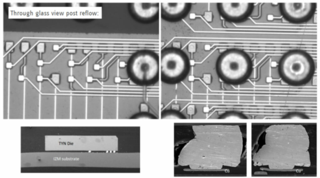
Assembly of Si PICs to glass substrates using laser assisted bonding, processed developed by ficonTEC Ireland. Si PICs and glass substrates developed by Tyndall & IZM, respectively
Machine optimization & process development for micro-optics assembly
ficonTEC additionally benefitted from working with an international corporation that was interested in learning about the micro-optical assembly processes first developed as part of DTIF. The manufacturing pilot line laboratory has also attracted visitors to the lab, boosting awareness of ficonTEC’s capabilities.
According to the feedback so far, the collaboration of academic and industry work, establishing a manufacturing pilot line has been advantageous in order to pass from TRL4-5 (research outputs) to TRL7-8 (pilot production). This also enables many companies in the country to approach the Pilot Line to discuss potential pilot production of their projects, benefiting Ireland.
ficonTEC Ireland
PIXAPP (completed)
The world’s first open-access
Photonic Integrated Circuit (PIC) Assembly and Packaging Pilot line
Consisting of a highly interdisciplinary team of Europe’s leading industrial & research organizations, PIXAPP’s goal is to help exploit the breakthrough advantages of PIC technologies by providing users with single-point access to PIC assembly and packaging.
In avoiding what is probably the most significant bottleneck in developing competitive photonic devices, the challenge is to create accepted design rules and standards for photonics packaging, including automatization of the processes and of mass-scale testing, so as to reduce the overall cost of PIC-based products.
By loading the video, you agree to Vimeo's privacy policy.
Learn more
The PIXAPP initiative covers five main aspects: design, materials, devices, applications, and equipment. ficonTEC’s role within the project is to target improvements and innovations of existing and future photonics assembly and testing equipment.
PIXAPP was a Horizon2020 ICT 2016 funded project and ran until the end of 2020.
Lasclad (completed)
Automated strip-&-cleave of optical ribbon fibers
The increased demand of photonic components worldwide and optical fibers and fiber ribbons in the photonics industry in particular leads to a demand for automated preparation solutions of optical fibers inside fully automated micro-assembly equipment. The goal is to achieve high reproducibility, high optical quality and high parts yield, while using alternative approaches for preparing fibers compared to manual fiber preparation.
Within the Lasclad project, a machine-integratable solution for an automated strip-&-cleave module was developed, including an automated CO2 laser-based process for a optical 12-fiber ribbon. Proof of concept has already been achieved. Further process optimization will improve the mechanical and optical quality and speed even further.
The development of this project is done in close collaboration between ficonTEC, Nyfors Teknologi AB in Stockholm, Sweden and the Fraunhofer Institute for Applied Optics and Precision Engineering (IOF) in Jena, Germany. The work was funded by the Eurostars Programme under grant #E!11443 Lasclad, together with financial support from the German Federal Ministry of Education and Research (BMBF).
UPDATE: The results topic has been demonstrated in our webinar on Fiber Assembly, where we also present a concept for a complete system capable of the entire fiber ribbon production workflow. Development of this capability is continuing further together with Fraunhofer IOF.
LaReBo (completed)
Laser-assisted low-stress reflow bonding of opto-electronic components
LaReBo was an investigation of a laser-assisted reflow bonding process for photonic components. The aim was to increase accuracy and component density, thus enabling smaller package sizes and so address novel products and new markets. The enabling technology is transmission laser-soldering with an absorption of laser radiation localized to the bond zone. Process knowledge was generated for automated bonding complete with an integrated process chain from component to package, and destined for economic, high-throughput and high-yield manufacturing.
ficonTEC’s role within the project was to provide an appropriate bonding machine equipped with a laser-assisted soldering module.
LaReBo was a Horizon2020 eurostars project and ran until late 2018.
PHASTFlex (completed)
Fully automated, high-precision, cost-effective assembly for next-generation hybrid photonics
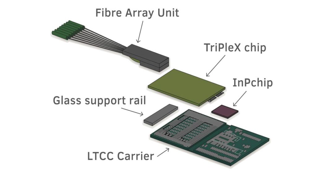
PHASTFlex proposed an innovative solution, in which InP PICs with active optical functions are actively aligned with passive, free-etched dielectric waveguide TriPleX™ PICs bonded onto an LTCC (ceramic) carrier, allowing a fine alignment of the waveguides in two lateral and one rotational axes. ficonTEC developed a unique assembly machine in which the coarse alignment of the chips on a common substrate as well as the active fine alignment of the waveguides could be performed in an automated assembly process.
The project’s goal was to develop a complete assembly process and the required tooling to implement this concept, including pre-assembly using eutectic bonding and automated handling, with on-chip micro-fabricated fine-alignment and fixing functions.
PHASTFLex was an FP7 funded STREP. It started on January 1, 2014 and was originally scheduled to run for 36, later 44 months.
Acknowledgment: phastflex.eu
Acknowledgment: phastflex.eu
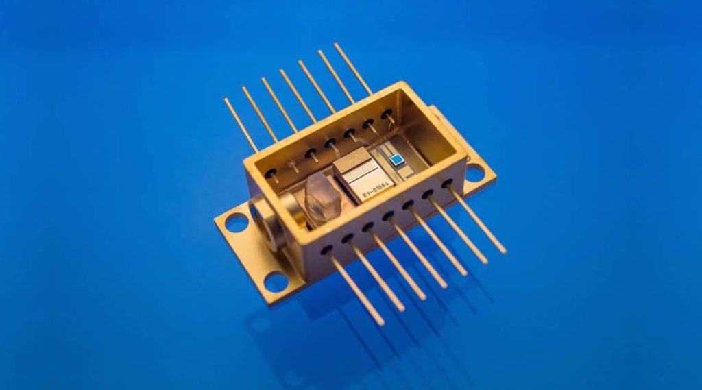
AutoFly (completed)
Automated assembly and bonding technology for
micro-optics and butterfly modules
The AutoFly project was initiated for the development of a fully automated, high-volume-capable process flow for the production of photonic devices. Core activities included development of innovative and automation-capable optical system approaches and concepts that additionally support the transition from manual to automated production. These approaches should be easily transformable into corresponding, fully automated assembly and attach technologies.
The project produced an automatically packaged 808nm laser module. The package can be hermetically sealed for application in harsh conditions. The high-precision mounting of a double-sided single lens with an innovative optical pick-&-place module was fully automated, with active alignment used to achieve a highly collimated and aligned free beam. This makes the system particularly suitable for sensor and interferometer applications.
AutoFly was a BMBF funded project and ran until 2015. Project partners were Fraunhofer IZM and eagleyard Photonics.