


Applications
Established and currently trending applications for photonics assembly & test
Since 2001 ficonTEC has been providing automated micro-assembly and testing solutions for the photonics manufacturing industry, in that time serving the needs of a broad selection of photonics-enabled segments.
Our machine solutions align-&-attach free-space optics, attach fiber pigtails, fiber arrays or waveguide couple to various types of light source, and assemble and test hybrid optoelectronic devices and high-power laser diodes. Our machine solutions perform regardless of the material system and of the device type involved, and independently of the target application. The underlying system architecture is scalable from early device development environments all the way up to high-volume production requirements.
With an installed base of over 1000 machines, our customers include THE leading integrated photonics components developers and suppliers around the globe. ficonTEC can supply assembly and test machines designed to achieve automated manufacturing in accordance with the latest device specifications in many sectors. These sectors include those noted below as well as much younger, only recently enabled technology sectors that seek to exploit photonics capability.
Telecom & Datacom
Photonics-enabled devices that manage content in the cloud and that move vaster amounts of data through the internet
Telecom (communications) and datacom (content transfer as well as management in the cloud) applications have long been the motivator behind the development of high-volume integrated photonics manufacturing. The essential drivers are the monetization of ever diverse online services, and the consumption of the related content via increasingly smart and capable networked devices.
Higher bandwidth, higher device density, greater energy efficiency (pJ/bit) and lower cost (US$/Gbit) in the devices that power these sectors can together only be realized through dedicated PIC approaches for their manufacture. This is in fact already reality – 100G and 200G transceiver manufacturing is now, 400G is getting very close, and next up is 800G and the 1Tb barrier.
In 2001 ficonTEC introduced a machine that automated pigtailing of AWGs (Arrayed Waveguide Gratings) and since then has gained extensive experience in these sectors, including the assembly of TOSA/ROSA, and later more complex (coherent) optical interconnects. Today, ficonTEC systems have assembled a significant share of the optical communications devices currently in use, and with co-package-capability already built-in with the new in-line platform, ficonTEC is well placed to continue this trend, as well as supporting 5G infrastructure development en route.
Naturally, all appropriate devices have to be assembled, packaged, and must then satisfy very rigorous, often proprietary testing procedures.

The following capabilities are of particular relevance to this sector:
- photonic device assembly & testing
- functionalizing devices with light sources, modulators, receivers & detectors
- hybrid optoelectronic device and flip-chip assembly
- I/O connectorization for fiber optics & waveguides
- combined electro-optical mixed-signal testing
- testing to very stringent (and varying!) standards
- high-volume capability involving high levels of automation
Relevant ficonTEC product lines include:
ASSEMBLYLINE, CUSTOMLINE, TESTLINE and WAFER TESTLINE sytems
Learn more
Low-power And High-power Laser Diodes
Where would we be without laser diodes and the myriad photonic devices that are made with them?
Laser diodes in various forms constitute one of the most important and prevalent components within the photonics sector. Initially discovered in the early 1960’s, the last 20 years in particular have seen a massive diversification of laser diode applications, with wavelengths spanning the entire optical spectrum and beyond, and with optical power ranging from mW to kW.
In the low-power regime, applications include low-cost laser range finding for autonomous ‘things’, laser-based approaches for metrology, analysis and sensing, VCSEL sources embedded into silicon photonics chips, laser emitter arrays for short-range lidar and 3D spatial mapping and recognition. At high powers the focus moves to materials processing in all forms – marking, welding, and cutting – and to laser pump applications.
ficonTEC has been supplying solutions for laser diode assembly, testing and characterization since 2004. Our machines can handle single emitters, or stack/unstack or bond multiple laser diodes and bars. They can also align free-space optics, attach fiber pigtailing or waveguide coupling, can mount fiber arrays to laser arrays, and are also certainly no stranger to automotive lidar and facial 3D mapping applications.
The following capabilities are of particular relevance to this sector:
- AOI (inspection) for chip facet inspection
- precision assembly for single emitters
- accurate & reliable stacking of laser bars
- free-space optics or fiber-optic coupling
- hybrid device assembly for multiplexed emitter devices
Relevant ficonTEC product lines include: ASSEMBLYLINE, CUSTOMLINE, TESTLINE, and STACKLINE systems
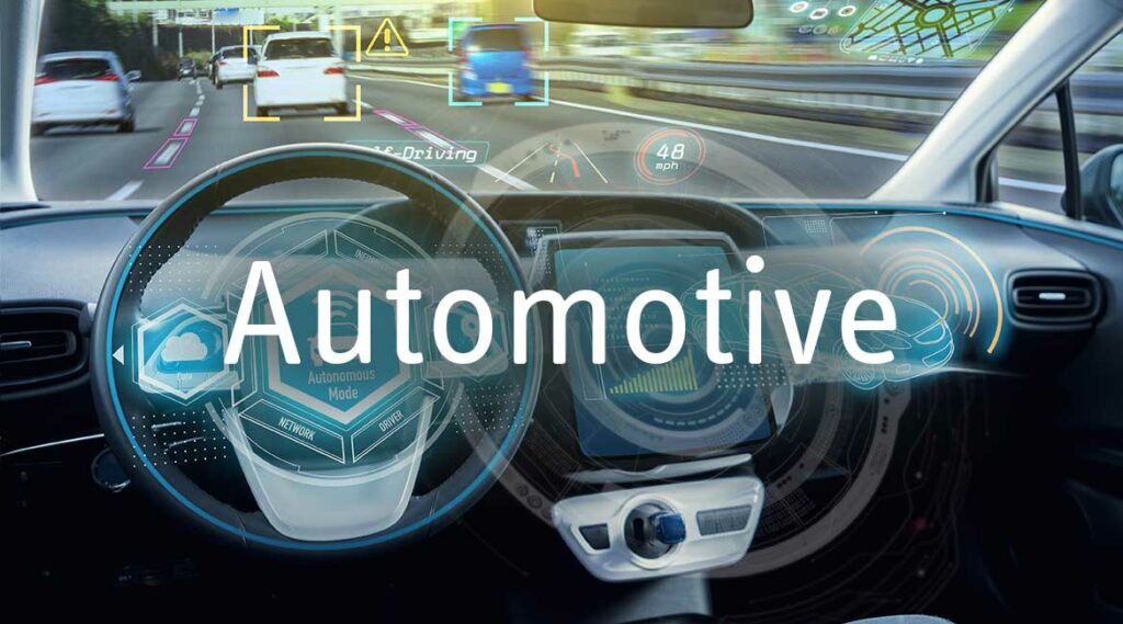
Learn moreAutomotive Lidar, Cameras and Lighting
Breaking new ground with manufacturing solutions for optical-based sensors and lighting, with applications in automotive and other sectors
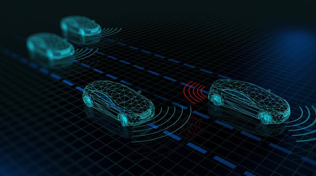
The automotive sector is undergoing two, maybe three major transitions – the electrification of the drive system, the implementation of automatic safety systems based on vicinity and hazard awareness, and ultimately the introduction of autonomous vehicles at various levels of transportation.
The near-term goal of integrating diverse optical sensing systems into automotive vehicles has kicked off a boom in camera and sensor development, perhaps the most prominent being lidar. All of these will eventually feed into the many driver assistance and safety systems now being touted – gesture sensing, pending hazard assessment, object recognition systems, automatic lighting adjustment, rangefinders for active cruise control, etc.
Various integrated photonics based devices provide a future-proof pathway to realizing efficient solutions for these needs. ficonTEC systems already provide the full gamut of capabilities required to assemble, package and test such devices.
Many of these devices are photonics-based, utilizing detectors, cameras, optics, LEDs, and lasers. As a whole, this sector is expected to grow with a CAGR of some 94% and reach US$2.3 bn by 2026. Significantly, device use is not only restricted to the automotive sector – lidar, for example, has additional critical industrial applications in aerial mapping, urban planning, and environmental monitoring.
With various announcements made on LinkedIN this year (2023) indicating the allocation of staff and resources internally as well as the participation in recent AutoSens events and others, it is clear that ficonTEC is targeting these new areas of industrial manufacturing.
Meet ficonTEC at upcoming events, including #automotive and #lidar. See the list here.

ficonTEC’s contribution to the sector
In the dynamic landscape of technology, lidar has emerged as an indispensable component in applications ranging from autonomous vehicles to environmental monitoring. As the integration of lidar sensors into various sectors continues to surge, the requirement is emerging for efficient, accurate, and scalable assembly, testing and calibration solutions.
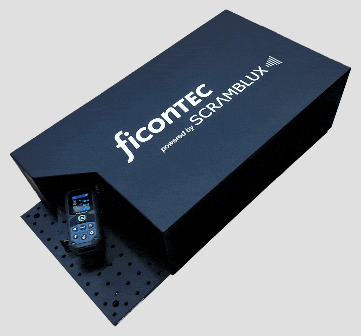
ficonTEC has recently set out together with start-up Scramblux GmbH to provide volume production solutions for automotive lidar, camera and lighting. In particular, three specific task areas come together to form a unique modular approach to the proposed production solutions:
- PiC testing, packaging and assembly
- optical and mechanical lidar assembly
- lidar end-of-line testing
For the last item above, the requirement for lidar end-of-line testing, Scramblux offers its BeamScrambler, an advanced optical measurement tool specifically designed for testing and calibrating lidar sensors across a wide range of performance parameters.
The following capabilities are of particular relevance:
- photonic device assembly for camera modules and emitter/detector devices
- LED array & laser module assembly for exterior lights and sensor systems
- hybrid device assembly for VCSEL/fiber-optic array coupling
- combined electro-optical mixed-signal as well as end-of-line system testing
- diode laser and photonic device characterization / verification
Relevant ficonTEC product lines include: ASSEMBLYLINE, TESTLINE, WAFER TESTLINE and STACKLINE systems.
BioMedical Testing
At the point of fusion between biotechnology, photonics, micro-fluidics and electronics
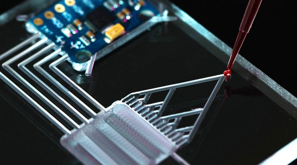
At the point of fusion between biotechnology, photonics, imaging, optofluidics and electronics, biomedical diagnostic approaches based on optical technologies are playing an increasing role in so-called personalized point-of-care solutions in the health sector. The advantages, both for the health care sector and for the patient, lie in the speed of diagnosis, that they are minimally invasive, and in the sensitivity and specificity provided. In some cases, these devices empower the patient with self-testing, with data collection and diagnosis being performed remotely.
For diabetes, blood pressure, and general health monitoring, DNA sensing, OCT engines, minimal invasive diagnosis, and many other ‘smart health solutions’, the requirement is for reliable and capable photonic biomedical devices that satisfy the very specific requirements of the health care industry.
The following capabilities are of particular relevance to this sector:
- photonic device assembly for OCT and biomedical sensing
- hybrid device assembly for optofluidic/electronic devices
- combined electro-optical mixed-signal testing
- catering to specific biophotonic device characterization and qualification
The greatest challenge for this sector is the achievement of functional photonic components (predominantly) in the visible range. For this, the initial goal for existing initiatives is to mature a SiN waveguide platform with very low propagation losses, low auto-fluorescence and a high level of integration. Additionally, some of these devices are designed to be ‘single use’, so must be correspondingly cost effective in their manufacture.
Relevant ficonTEC product lines include: CUSTOMLINE, TESTLINE, WAFER TESTLINE, and LASER WELD systems
Learn moreInternet of Things
Assembling and testing the photonic devices located at the edge that make more ‘sense’ of the world around us
The term ‘Internet of Things’ (IoT) commonly refers to networked sensor devices that, due to the many optical approaches utilized within them, represent yet another major convergence for sensing and photonic technologies, and again an applications space with significant growth potential.
These networked devices can see, smell, count, analyze or in some other way ‘sense’ the local environment and thereby contribute to an accumulation of data that can be used to address a variety of societal needs – traffic data for autonomous vehicles and for traffic flow analysis, assorted household management systems, weather data acquisition and e.g. flood prediction, roadside and industrial air pollution monitoring, farm and crop management, etc.

The following capabilities are of particular relevance to this sector:
- photonic device assembly for environment sensing
- hybrid device assembly for multi-emitter/detector devices
- optically/electronically-connectorized devices to enable remote interrogation
- combined optical-electronic testing
- device characterization to diverse specifications
More devices means more sensors means more photonics components. And if they are to be energy efficient and exhibit low device cost, this in turn means greater use of integrated concepts in device approach and greater adoption of advanced automation in their manufacture – in many cases at high volumes. It also means more networked data, which ultimately feeds back into the growth of the telecom, datacom and 5G sectors.
Relevant ficonTEC product lines include: CUSTOMLINE, TESTLINE, WAFER TESTLINE, and LASER WELD systems
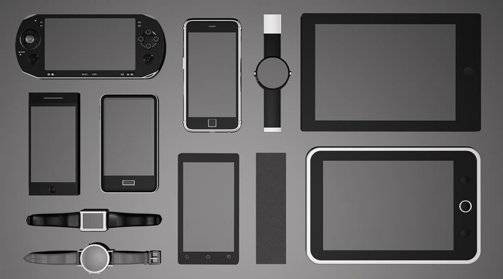
Learn moreConsumer Electronics
Assembling the photonics components and devices that empower consumer electronics technology
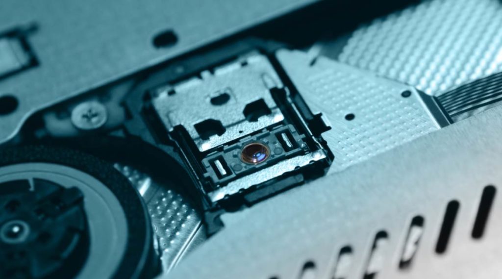
Improvements in optical device manufacture (efficiency, miniaturization, high-volume) enable increasingly ‘smart’, capable and cost-accessible consumer electronics. From smart refrigerators, to gesture-controlled TV sets, devices for the watch industry, and on to retina displays and facial recognition in smartphones – these all rely in part on optical technologies to provide visual performance or multiple sensing and tracking capabilities.
Modern compact dual camera modules in smartphones provide 3D capability, embedded VCSEL arrays and diffractive micro-optics provide 3D object recognition, micro-displays powered by super-luminescent LEDs, optical sensors in watches and other ‘wearables’ monitor heart rate, blood sugar and other parameters. The list goes on – and all of these devices will become increasingly compact, efficient and capable.
The following capabilities are of particular relevance to this sector:
- photonic device assembly for short-range sensing
- hybrid device assembly for multi-emitter/detector devices
- assembly & bonding to ‘consumer’ requirements
- combined optical-electronic testing
- device characterization within very different parameter framework
ficonTEC has been continuously involved in photonics integration developments for many years. Today, we are actively collaborating with technology leaders to develop innovative assembly and test processes that are effective across all material systems, and thus also at all practical (integrated photonics) wavelengths. As PIC technology gains breadth, better standardization and greater accessibility to integrated photonics manufacturing approaches – including assembly, packaging and testing – will help drive take-up in consumer applications.
