


Moving to high-volume wafer-level assembly by accelerating the transition from singular and discreet, to many being processed in parallel
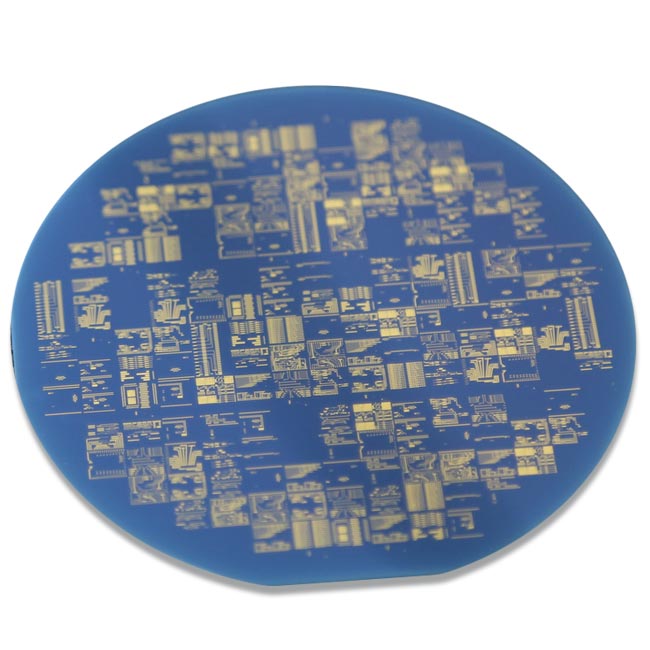
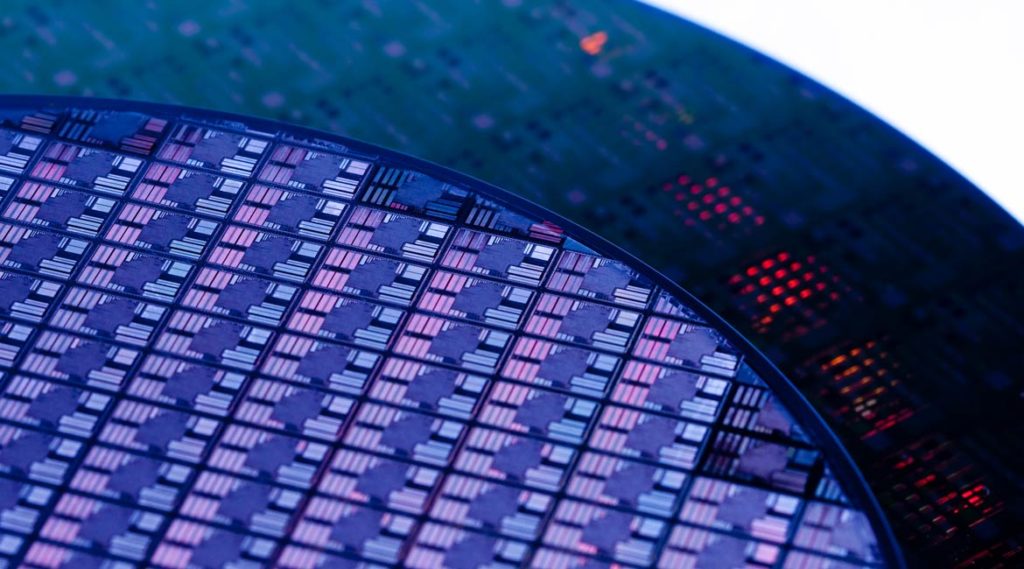
For a number of applications, photonics micro-assembly technology is currently undergoing a transition to a ‘micro-chip’ approach, much as that experienced by the electronics industry some four decades ago. Multiple functionality and components are integrated onto a single chip or a small hybrid chip assembly, utilizing so-called photonic integrated circuits (PICs), and where the underlying ‘design for manufacturing’ technologies have been shaped by the need for fully automated, high-volume manufacturing – instead of production in the 100s & 1000s, PIC approaches are designed for numbers in the 100,000s and millions.
This in turn means the adoption of wafer-level or at least in-line processes, both in assembly and in testing, and where equipment amortization is no longer measured via initial capital investment, but in cost/part.
Acknowledgment: By JonathanMarks (Own work)
CC BY-SA 4.0, Wikimedia Commons
Where Are We Now?
Integrated photonics components are poised to experience rapid acceptance and growth, across diverse applications
Acknowledgment: By Ehsanshahoseini (Own work)
CC BY-SA 4.0, Wikimedia Commons
Over the last decade or more, there have been a number of international initiatives and projects that have addressed a number of different requirements, issues and goals surrounding implementation of varying PIC technology approaches. There are, for example, differing material systems that are individually best suited to specific optical tasks, there are standards issues regarding interfacing and testing that need to be addressed, and there are design-kit environments that need to be developed to safeguard capability and interoperability across diverse fab environments and services. In short, the complete eco-system
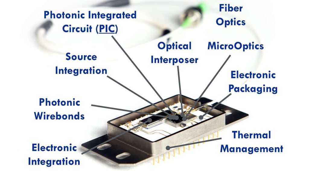
Naturally, assembly and testing are equally critical aspects of the PIC technology implementation, and ficonTEC has already long-served budding PIC applications with various stand-alone machine solutions. Additionally, supported by an active R&D team engaged in prominent international research initiatives, ficonTEC has played, and continues to play an active role in helping to develop a proper understanding of what the assembly, packaging and testing requirements of the manufacturing industry will actually be.
Now, with a next-generation, configurable machine platform introduced in early 2019, we are addressing growing interest in more sophisticated and reconfigurable machine systems. On the one hand, specific ‘standard’ in-line machine configurations can be supplied as individual and versatile production cells for existing production lines. On the other, multiple machines can be supplied as a task-optimized production segment comprising several differently configured systems. In principal, even entire production lines can be envisaged.
Following product retirement, these systems can then be re-configured and re-purposed. Our long-term and on-going machine design strategy thus already enables an in-line, high-volume automated approach to photonics assembly and testing, with flexible options for re-use for other applications.
Acknowledgment: pixapp.eu
What Is The Way Forward?
Understanding how the assembly and testing needs of industry will change over the next ten years
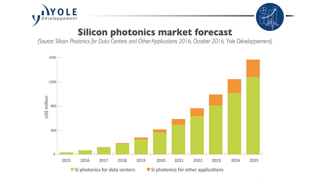
The market forecasts for integrated photonics applications are very positive, with CAGR expected to be somewhere in the region of 20 to 30% until 2025 and beyond. For telecom (communications) and datacom (big data, cloud services), this development is already very real. For all other photonics applications, with improving PIC access and capability, interest and diversity of application are snowballing. The way forward for photonics integration is no longer a question of ‘if’ but is instead one of ‘how soon’.
A move to higher levels of photonics integration is associated with the need for increased miniaturization, higher yield, and better standardization all the way from early photonics design, to prototyping and through to assembly and testing. All leading to a lower cost/part at both low and high volumes.
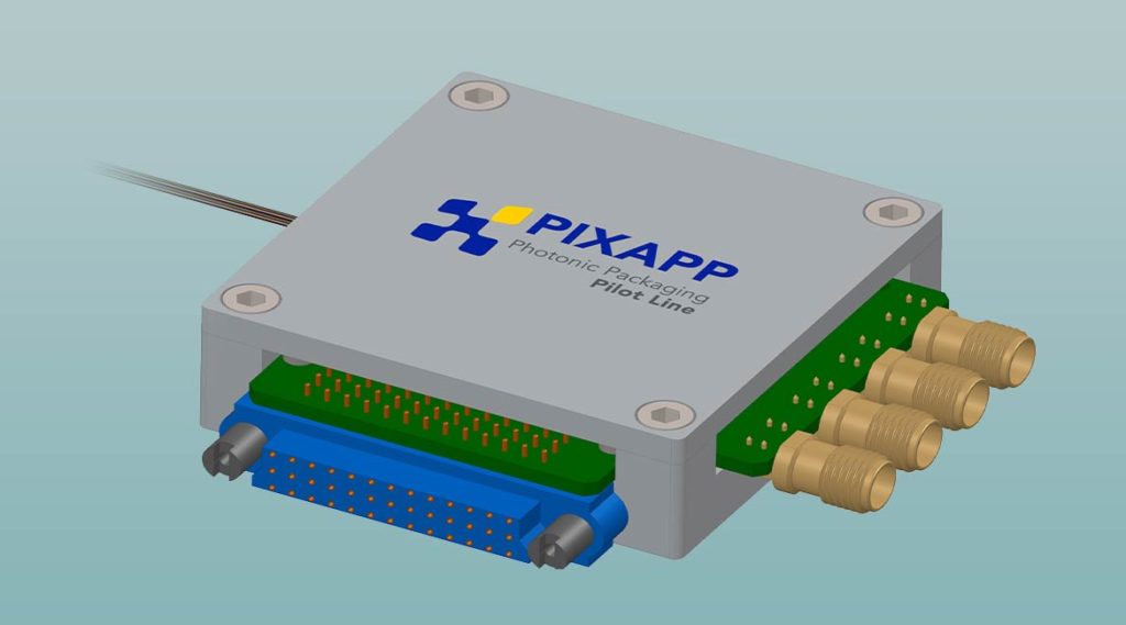
Photonics is poised to be the next semiconductor frontier, from consumer to high-power computing. ficonTEC’s own contribution to the way forward is advanced automation, having already gained valuable experience through the successful completion of comparable solutions for PIC applications with existing clients. Nonetheless, the company still takes an active and continuing role in current international Projects & Initiatives – such as PIXAPP – that are designed to provide both infrastructure and ease of access.
ficonTEC
Acknowledgment: pixapp.eu
By better understanding the developing needs of the greater photonics community in this area as early as possible, the goal is to be able to provide the solutions as and when they are required.
