


Over 1000 machines delivered and installed globally, each shaped by the needs of the customer and the application
Since its original founding in 2001, ficonTEC has become the market leader for individually customized solutions for semi or fully automated micro-assembly and testing of opto-electronic components, micro-optic assemblies and photonics-enabled devices.
Our machines employ industry-proven production technologies – micro-positioning, active/passive precision alignment, attachment via welding, soldering and/or bonding, and automated optical inspection. ficonTEC also provides a suite of test capabilities for individual components and hybrid optoelectronic devices, both on and off-wafer. Moreover, with everything being orchestrated by our flexible PROCESS CONTROL MASTER software, the machine platforms and product lines described below become so much more than just the sum of their parts.
The technologies and capabilities implemented in all machine platforms translate into a broad and established spectrum of production process expertise. We are continually refining capability, modularity and design so that these systems reliably and cost-effectively meet and exceed efficiency and yield requirements even for cutting-edge production processes. For the team here at ficonTEC, these are the challenges we face every day.
Product Lines
Functional machine types designed to accomplish class-leading flexibility, speed and results in photonic device production
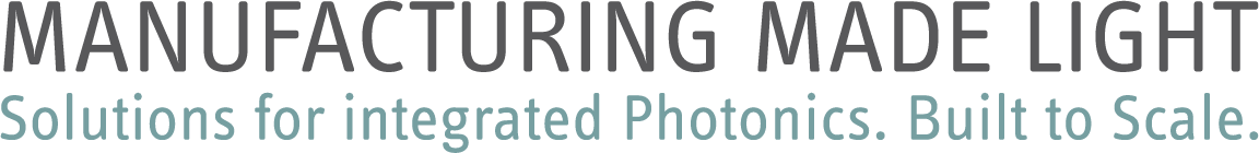
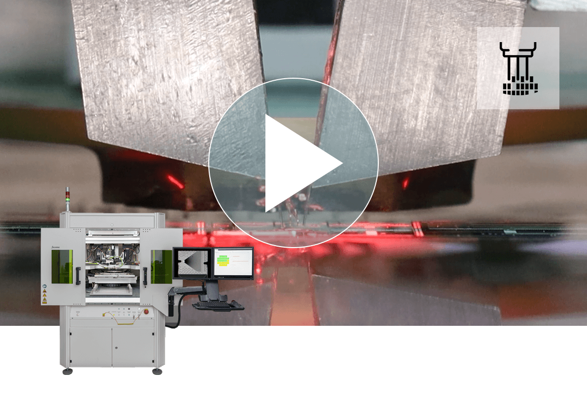
ASSEMBLYLINE
Automated die-level photonic device assembly
Fully automated, industry-qualified assembly for optoelectronics and singulated photonic devices and PICs. Featuring high-precision ‘align-&-attach’ bonding capability for all optical elements, fibers and arrays, as well as for die, chip or PIC integration and hybridization.
Read More
ASSEMBLYLINE systems are fully automated ‘align-&-attach’ assembly systems for the production of optoelectronics and photonic devices. They uniquely combine high-precision optical alignment capability with epoxy-based attachment, eutectic die bonding and/or laser soldering for all optical elements, waveguides, fiber types and die, chip or PIC hybridization tasks – all in an industry-proven design.
These assembly systems are available as individual, versatile, and highly capable stand-alone cells, or as highly specific in-line process cells for insertion into existing production lines. Optional modules provide additional features, including automatic tool changing, wafer handling capability and TESTLINE (test-&-qualify) functionality.
ficonTEC’s next-generation system architecture is designed to be production-line-capable from the ground up. By utilizing state-of-the-art handling and feed in/out options, task-optimized ASSEMBLYLINE and TESTLINE systems can be combined in an extended line configuration for volume manufacturing. Optional, ML-based process monitoring hardware and software add-ons ensure minimal downtime.
N.B. – From Q2 2022, former ASSEMBLYLINE, BONDLINE & FIBERLINE products have been rolled into a single ASSEMBLYLINE line-up
Key features
- High-precision motion referencing and alignment
- Pick-&-place from/to standard/custom carrier formats
- Fully automated passive & fast-active ‘align-&-attach’
- Epoxy and eutectic bonding, laser soldering
- For all optical element, fiber, chip, PIC & custom assembly tasks
- OCR-compatible for component traceability
Tasks & applications
- All optical element & chip-on-XXX ‘align-&-attach’ tasks
- Fiber & waveguide assembly/pigtailing/connectorization
- Adaptable to high-complexity co-packaged applications
- For FTTX transceivers, HPLD modules, hybrid integration, MOEMS, PICs, silicon photonics, co-packaged devices sensors and lidar, transport, IoT and 3D scanning
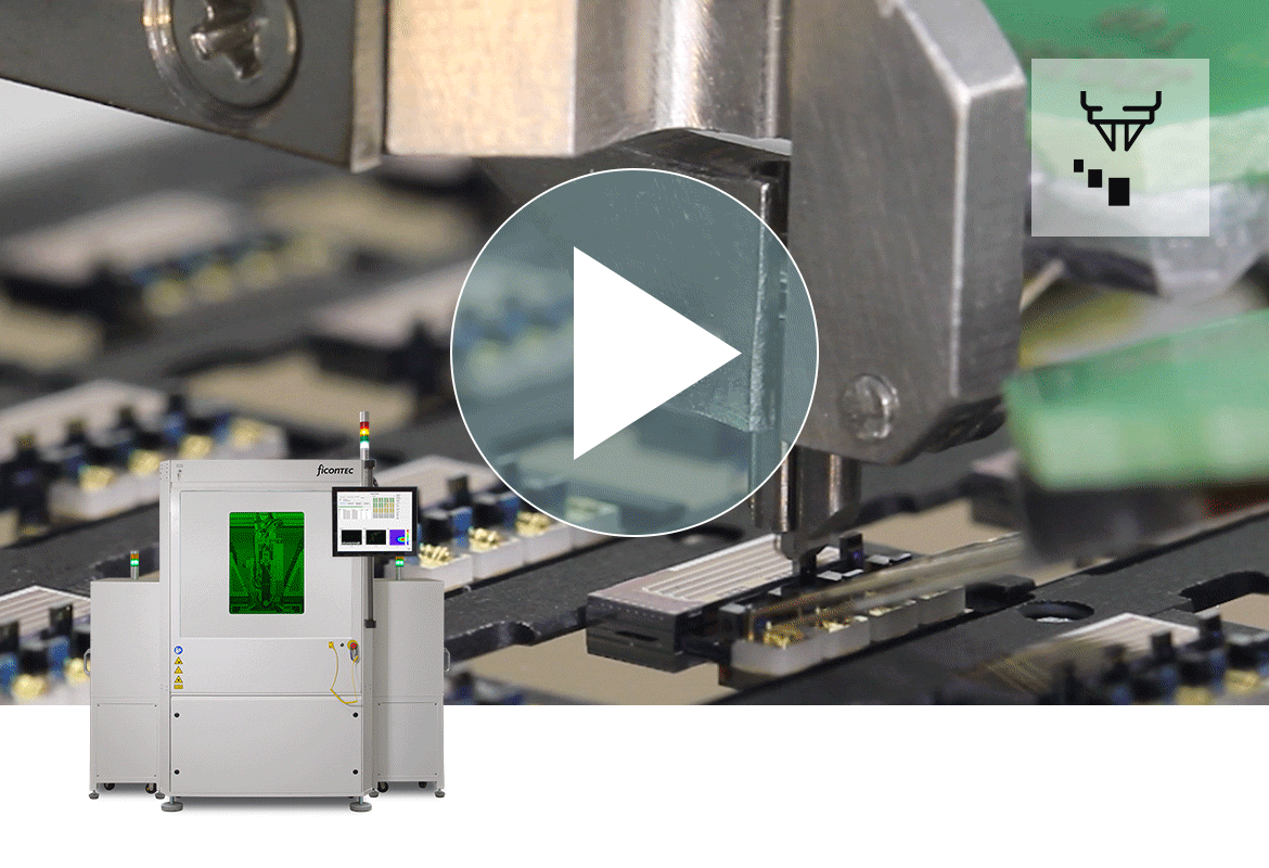
CUSTOMLINE
Flexible, multi-purpose ‘align-&-attach’ platform
A highly capable development and/or batch processing platform, uniquely combining high-precision optical alignment capability with a multiplicity of bonding technologies. Designed for all optical, fiber and die/chip/PIC connection and hybridization tasks.
Read more
CUSTOMLINE is a highly capable development and/or batch processing platform for customers in the semiconductor and photonics packaging market. More than any other ficonTEC product, these systems combine high-precision optical alignment capability with a multiplicity of assembly technologies – including epoxy-based attachment, eutectic die bonding and laser soldering.
Available as a versatile and stand-alone assembly cell, and with the broadest array of installable modules for any ficonTEC platform, CUSTOMLINE can be configured – and re-configured – to the widest range of R&D, process development and batch manufacturing tasks. Extensively utilized in academic and collaborative research as well as in photonics jobshop environments, CUSTOMLINE is an industry-proven design.
Importantly for any development process, CUSTOMLINE systems can be operated manually, semi automatically or fully automatically. Optional modules extend functionality even further, including automatic tool changing, wafer handling capability and Testline (test-&-qualify) functionality.
Key features
- High-precision motion and alignment (µm/sub-µm)
- Pick-&-place from/to standard/custom carrier formats
- Epoxy and eutectic bonding, laser soldering
- Heating plate, bond force and flip-chip modules
- Exploratory R&D through to batch production
Tasks & applications
- Optical element & die/chip/PIC ‘align-&-attach’ tasks
- Fiber & waveguide pigtailing & connectorization
- Transceiver, co-packaging & hybrid development
- Flexibly configurable with TESTLINE capabilities
- Development and batch manufacturing for sensors and lidar, communications, transport & IoT, and 3D scanning
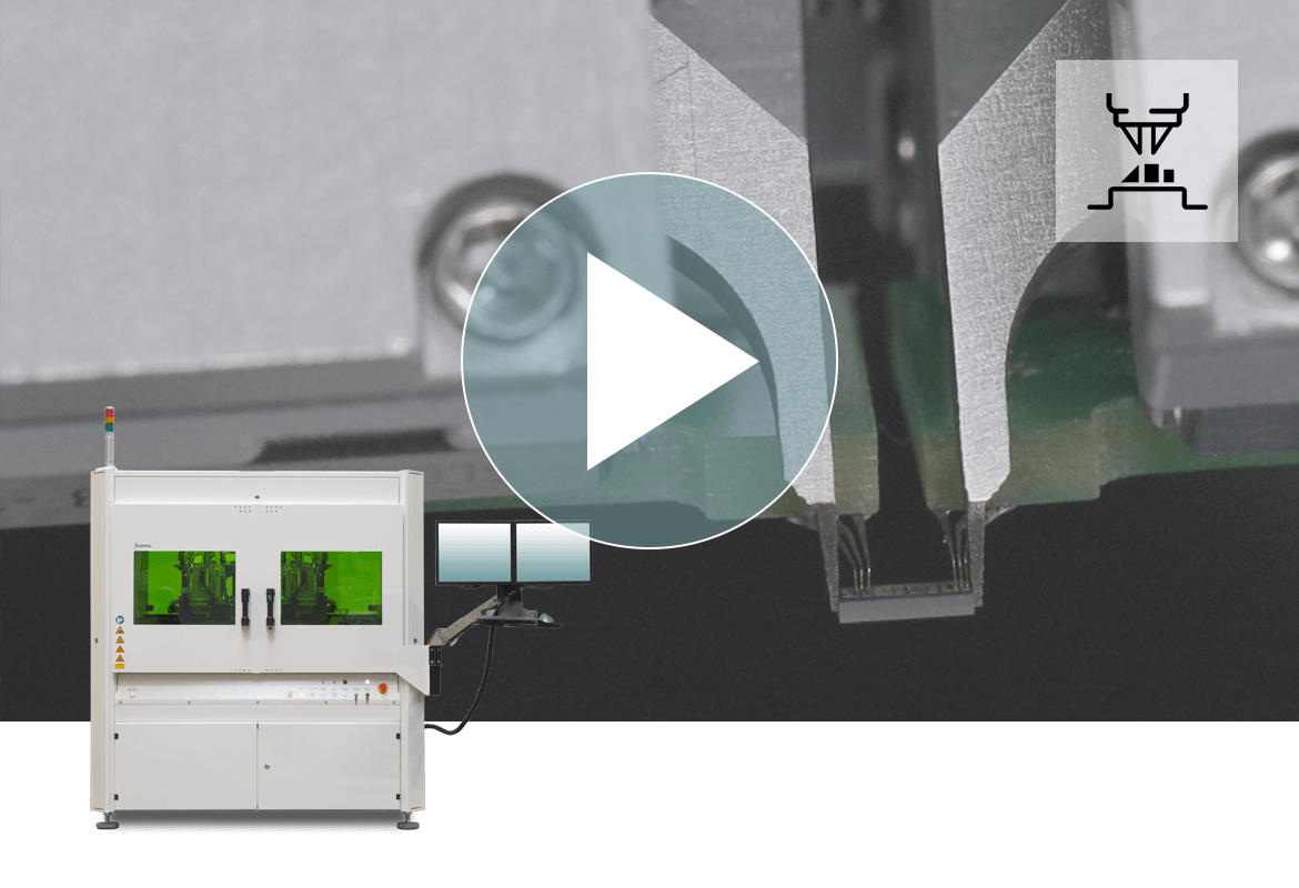
TESTLINE
Fully automated die-level photonic device test
Fully automated, mixed-signal electro-optical test systems for optoelectronics and singulated photonic devices. Featuring DC, RF and optical measurements in a production-optimized modular layout, and targeted at R&D, volume manufacturing, and anything in between.
Read more
TESTLINE production systems are fully automated solutions for electro-optical testing of optoelectronic devices and of singulated PICs (passive/active). Other complex tasks include LIV, spectral and near/far-field beam characterization of single laser chips (incl. VCSELs), unmounted laser diode bars and chip-on-submount (CoS) sources. Lastly, TESTLINE systems can be routinely equipped to also perform detailed optical facet inspection using Deep Learning for defect recognition.
Stand-alone systems are designed to provide as much multi-functional test-&-qualify capability as possible and are best suited to complex testing requirements requiring multiple capabilities within a single machine. This makes the stand-alone systems ideal for test development and for batch processing requirements.
ficonTEC’s next-generation in-line system architecture is designed to be production-line-capable from the ground up. By utilizing state-of-the-art component handling and feed in/out options, TESTLINE and ASSEMBLYLINE systems can be combined in a task-optimized production line configuration to provide volume-capable manufacturing.
N.B. – From Q2 2022, former InspectionLine products have been rolled into the new Testline products
Key features
- High-precision motion referencing and alignment
- Pick-&-place from/to standard/custom carrier formats
- Die-level handling, testing, and sorting as required
- Fiber alignment to I/O ports (arrays) in max. 4s
- Low-loss I/O port coupling with < 0.4 dB repeatability
Tasks & applications
- Rapid R&D, in-line & end-of-line device testing
- Optical facet inspection with AI defect recognition
- Test-&-qualify of chips, single emitters, laser bars, PICs, silicon photonics, hybrid devices
- Applications in telecom/datacom/5G, sensors and lidar, transport & IoT, 3D scanning & healthcare
WAFER TESTLINE
Fully automated electro-optical wafer-level device test
Innovative mixed-signal electro-optical test systems for non-singulated photonic integrated circuits (PICs) and other optoelectronic devices. Featuring fully automated DC, RF and optical measurements both on-wafer and for single photonic devices on appropriate carrier formats.
Read more
The WAFER TESTLINE product line is specially designed as a versatile electro-optical test-&-measurement system platform for wafer-level photonic device test. A re-configurable probe-wafer layout even caters to multiple PIC designs on a multi-project wafer (MPW).
For R&D proof-of-concept device test tasks, WAFER TESTLINE provides state-of-the-art, multi-channel e/o test of on-wafer waveguide and PIC I/O. Custom 3D-printed fiber tips provide support for edge-coupling, so low-loss coupling is enabled for all optical coupling mechanisms.WAFER TESTLINE also works equally well for multiple singulated devices on appropriate carrier formats.
For volume manufacturing, all identical devices on a wafer can be tested fully automatically. Built-in device cataloging and traceability thus enable yield and performance data across entire wafers, resulting in extremely valuable and previously unattainable feedback for the wafer fabs.
Key features
- Automated I/O port referencing to sub-µm accuracy
- Vertical and edge alignment to I/O ports in max. 4s
- Low-loss I/O port coupling with < 0.4 dB repeatability
- Superior test data acquisition over manual approach
- Wafer fabs receive PIC yield data across entire wafer
Tasks & applications
- Automated test-&-qualify for passive/active devices
- Proof-of-concept and low-complexity volume e/o test
- MPW-capable due to adaptable probe-wafer layout
- Off-wafer device capable with suitable carrier formats
- Adaptable to high-complexity co-packaged applications
- For communications, sensors/lidar/IoT and 3D scanning
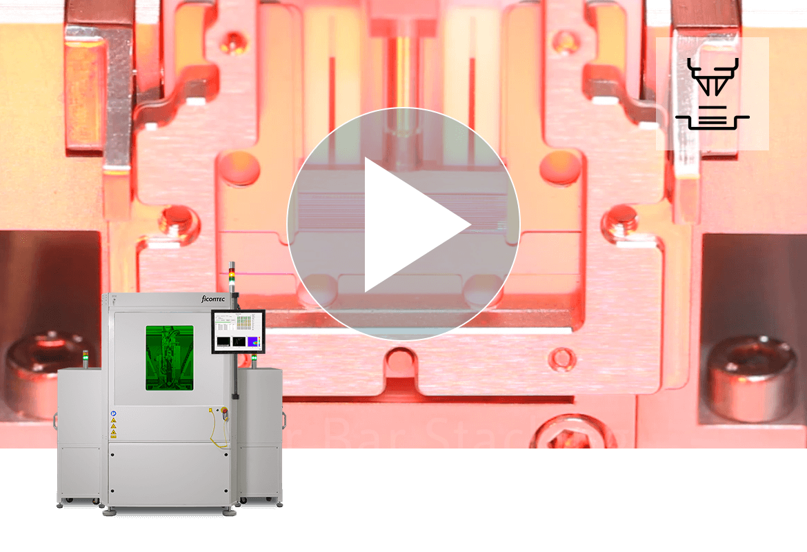
STACKLINE
Laser Bar Stacking
Fully automated precision stacking/unstacking for semiconductor laser diode bars. Typically used in preparation for a coating process, and/or for post-process unstacking and optical inspection of facet and side walls (optional). Configurable as a stand-alone or as an in-line assembly cell.
Read more
STACKLINE systems have been uniquely designed to provide fully automated device stacking and/or unstacking capabilities. This is realized by drawing together selected capabilities from the ficonTEC packaging toolbox – our ubiquitous machine vision system referencing and component recognition/handling, ASSEMBLYLINE’s passive alignment routines, and Testline’s AI-based defect recognition facet inspection procedures. Seamlessly managed by a common process-oriented control interface, the result is an industry qualified and flexibly programmable stacking/unstacking system that continues to see wide usage.
Stacking is typically required in preparation for coating (sputtering) processes, with subsequent post-process unstacking and inspection of facets and (optional) side walls. These systems are compatible with all high-precision, flush or staggered spacer diode bar stacking and unstacking needs. Although primarily available as versatile and highly capable stand-alone cells, they can also be configured as in-line process cells for volume production lines. The latest updates include optional, ML-based process monitoring hardware and software add-ons to ensure minimal downtime.
Key features
- High-precision machine vision motion referencing and alignment
- Pick-&-place from/to standard/custom carrier formats
- Nominal +/- 2 µm, optional +/- 0.5 µm alignment accuracy
- Optional dimensional checking and full facet inspection
- Integrated flowbox, electrostatic protection and Class 1 laser safety
Tasks & applications
- Stacking (flush/staggered) of bare singulated laser bars up to 20 mm
- Device sorting from singulated wafers
- Unstacking from, and inspection of coated LD stacks
LASER WELD
An automated microwelding station for photonics
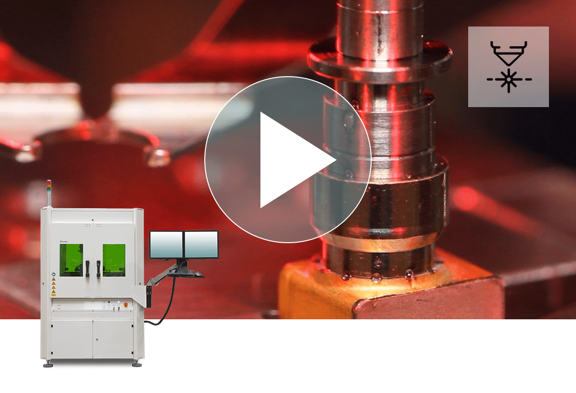
A 2 or 3-beam vertical configuration, laser microwelding machine cell utilizing a fiber-coupled Nd:YAG laser and additionally featuring automatic alignment, device characterization, testing capabilities and sophisticated component tracking throughout the entire machine process.
Read more
LASER WELD systems are fully automated ‘align-&-attach’ microwelding production cells for photonics. These systems are typically used for optical assembly and for coupling light out of photonic device packaging (butterfly, TO, custom), using for example, either ferruled optical components or single/multi-fiber coaxial assemblies.
Comprising a vertical dual-stage layout, each stage has its own high-precision multi-axis movement. A 2-beam configuration enables direct fiber to chip coupling and confocal optical train assembly of miniature components in common package formats. A 3-beam configuration features 45° or 90° beam out-of-plane incidence for fillet or butt/lap-style welding of coaxial components, respectively.
The welding process can be performed on passive or actively driven components and can incorporate an optional inert gas feed for improved weld quality. Post-weld characterization and testing procedures enable performance and yield monitoring, with ‘post-weld shift’ correction capability available for ‘out-of-spec’ results.
Key features
- Fully automated 2 or 3-beam microwelding station
- Motion system precision and tolerancing for fiber alignment
- Precision goniometer angular control of the lower tooling stage
- Standard and custom device package tooling available
- LaserHammeringTM post-weld shift correction capability
Tasks & applications
- Suitable for all ferruled optical components and devices
- Fiber to chip, fiber to package, single or multi-fiber devices
- Coaxial laser diode modules, optical isolators, WDMs
- For terrestrial, aerospace and space satellite applications
Product Platforms
Platforms that bridge the gap from R&D, process development, and through to complex, high-volume and even multi-line in-line production
ficonTEC provides its machine systems in one of three production platform types – stand-alone systems, in-line-capable systems, and entry-level. Experience shows that the choice of platform and housing type is strongly dependent upon the application requirements as well as the short-, mid- and even long-term development and manufacturing needs of the customer. Only when these aspects have been made known and discussed does it make sense to specify a platform type.
ficonTEC has over 20 years of experience designing and producing diverse manufacturing systems – armed with the right inputs, you can rely on us to recommend the right configuration. Moreover, all platform and housing types can be re-configured after product end-of-life, and can thus be cost-effectively re-purposed for other (e.g. emerging) applications.
Entry-level systems
While more budget conscious, ficonTEC’s entry-level systems are still designed to provide results more representative of the more highly specified stand-alone machines. A small number of optional modules are available, and the capital outlay is low.
These units are primarily intended for laboratory use, R&D, low-volume proof-of-concept manufacturing and other low-complexity applications. Typical use includes align-&-attach of optical and optoelectronic components, fiber-optics and dies, for example to micro-optical packages or onto PICs or other chip substrates.
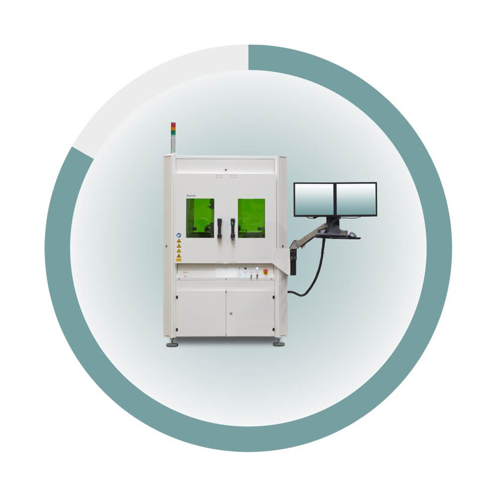
Stand-alone machines
Traditionally our most popular and industry-proven machine format. With world-class performance, comprehensive customization options, and exceptional real-world reliability, these machines are best suited to complex production requirements requiring multi-functional, multi-step assembly, bonding or testing capability within a single, stand-alone machine system.
Read More
The stand-alone systems traditionally utilized legacy machine housing designations, but from Q2 2022 these have now been brought up-to-date to better match the later in-line configurations. Larger systems are more easily feed-system-capable, and different feed and cassette philosophies can be implemented to best suit the exact application.
Suitable for: R&D all the way through to low-volume and batch manufacturing. Special purpose cells can be flexibly designed, and robotic systems incorporated to suit customer requirements. See individual product PDFs for more feature details.
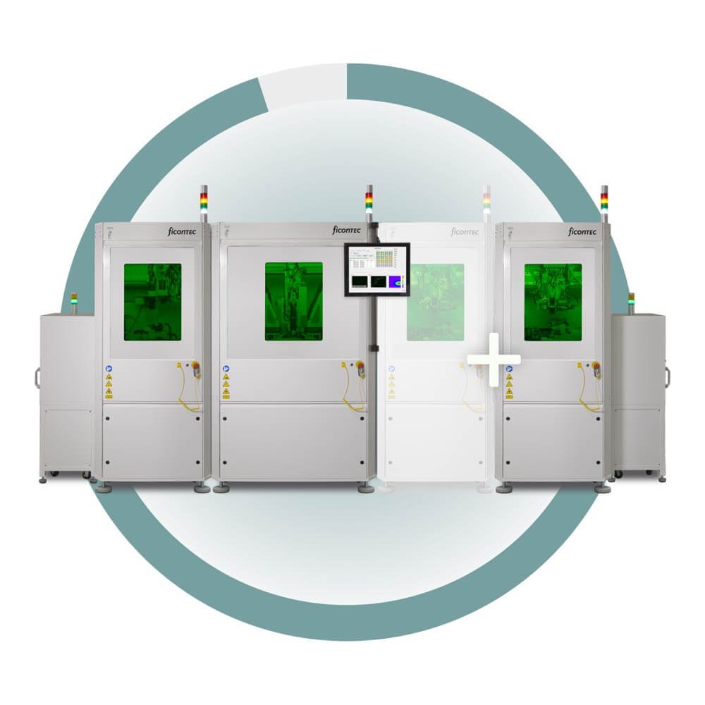
In-line machines
ficonTEC’s next-generation in-line machine systems feature improved modularity and more flexible feed-in/out options in order to be in-line-capable from the ground up. Utilizing a more modern housing format this platform addresses increasing industry demand for greater versatility together with higher volume manufacturing requirements.
Read More
This housing format can be supplied individually as versatile stand-alone production cells, or instead as highly task-optimized machine systems for production lines – singly, or as segments comprising several different machine types. In principle, even entire production lines can be envisaged, encompassing the full suite of processes required for photonics assembly and test.
Suitable for: R&D & NPI, cassette-to-cassette and in-line high-volume manufacturing, as well as for multiple production line set-ups operating in parallel and in sync. Special purpose cells can be flexibly designed, and robotic systems incorporated to suit customer requirements. See individual product PDFs for more feature details.
Don’t see what you are looking for?
Product designations are fluid, e.g. ASSEMBLYLINE systems must also often be ‘TESTLINE capable’, CUSTOMLINE can feature both active/passive assembly and test modules, and many systems can be made ‘wafer-capable’. There are also strongly trending applications for which our systems are already capable and are already in use – lidar, co-packaged optics, 5G infrastructure devices, through-silicon ‘align-&-attach’ are just a few.
