Capabilities That Set Us Apart
Innovative, industry-qualified manufacturing capabilities designed to
serve and exceed your production requirements
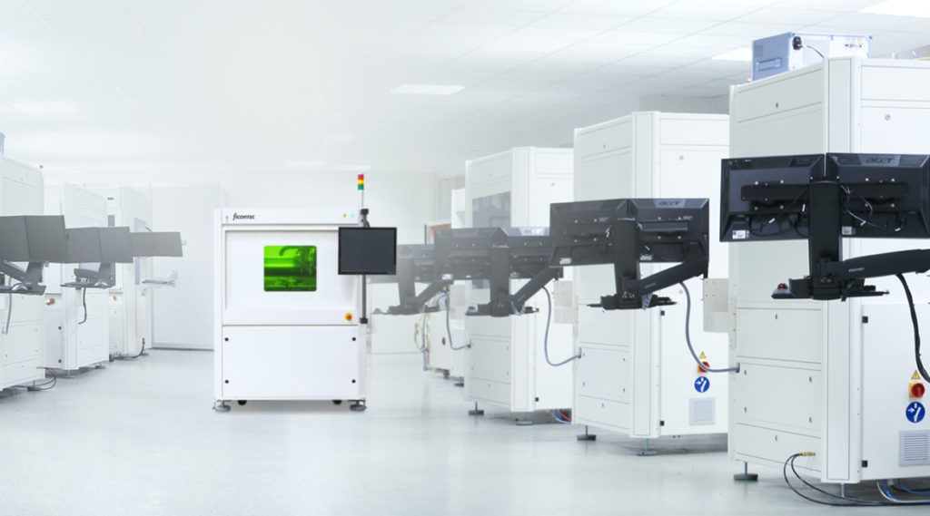
The technologies available to ficonTEC and implemented in the different machine solutions translate into a broad and established array of production capabilities specifically geared to provide the most efficient route to photonic device micro-assembly and testing. This is simply ‘Design for Manufacturing’ taken as far is currently possible.
Working closely with our customers and based on our broader expertise gained over 20 years of active development, the best capabilities for the application are determined. We take an active role in educating the customer to adopt these capabilities fully.
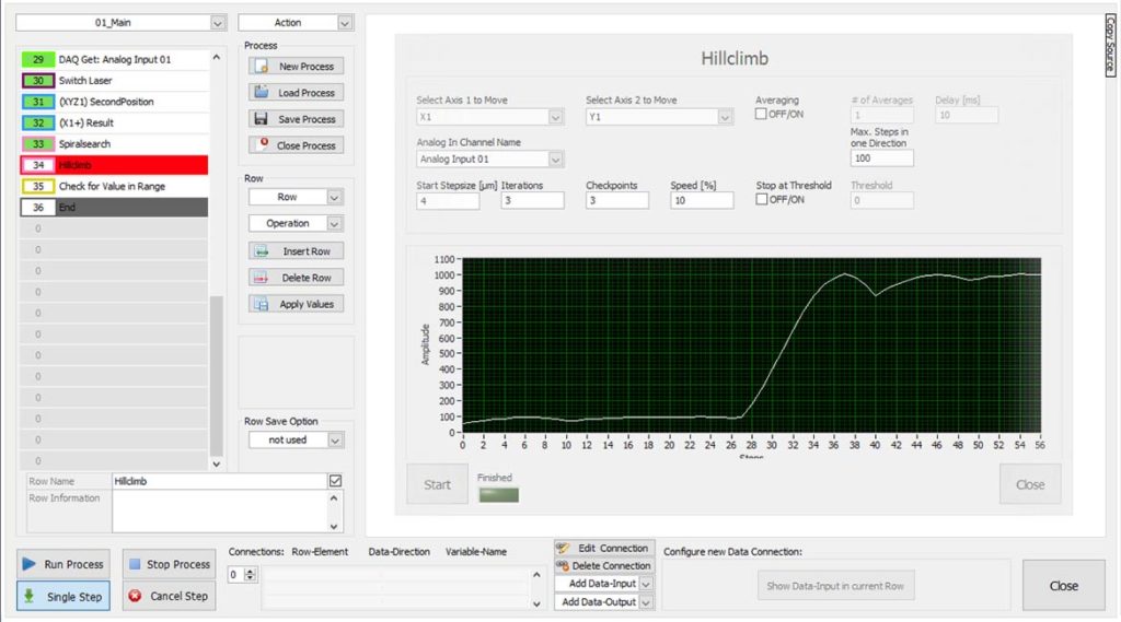
We assist in evaluating existing processes and methods, optimizing and developing innovative processes right through to their implementation, resulting in optimization of the assembly processes and thus achieving maximum production efficiency. The result is a turn-key system, with all hardware and automation functions controlled by ficonTEC’s flexible and easy-to-use PROCESS CONTROL MASTER application software.
This level of collaboration makes ficonTEC the ideal partner for a wide range of application spaces requiring advanced photonics assembly and testing solutions.
Learn more
Motion Systems For Passive & Active Alignment
Top-of-the-line high-precision positioning and advanced machine vision combine to form a fully referenced motion system
Multiple multi-DoF positioning systems provide flexibility, while AI-driven machine vision algorithms drive efficiency
Dual-fiber alignment to on-wafer waveguides
Our passive alignment routines rely on multiple camera systems and advanced machine vision algorithms that are seamlessly interfaced to motion control via automated geometric calibration procedures. Camera image space (pixels) can then be carefully calibrated to the actual motion space, up to the diffraction limit of the optical system, providing class-leading guidance, pre-alignment routines, and other advanced functionalities. Some of our alignment procedures are even completed in the IR.
Active alignment is usually an additional step following passive pre-alignment, and while slower, it used when sub-micron accuracy and repeatability is required. Here, a coupled optical parameter such as power is correlated with positioning in motion space. Nanometer-scale resolution can be achieved with piezo-driven stages, which utilize search trajectories that are pre-programmed into the motion control firmware.
Several aspects of optical component alignment are key to time-efficient micro-assembly:
- machine vision reduces active alignment search space, saving hugely on time
- efficient pre-alignment routines save time again and help guarantee yield
- automatic active alignment is possible regardless of the optical beam property, e.g. divergence, absolute optical power, spectrum, degree of polarization, splitting ratio, etc.
- minimal post-bond shift is ensured by ‘active tracking’ measurements and monitoring of the relevant parameters during the bonding process, together triggering any necessary positional correction of the optical elements.
Typical applications that require passive and active alignment steps include:
- fast active fiber alignment
- fiber pigtailing for edge-planar waveguide coupling
- single and arrayed fiber pigtailing for top-grating couplers
- fiber-optic cable assembly
- laser bar stacking and alignment of collimating micro-optics
- compact camera module assembly
… and many other opto-electronic alignment tasks.
Sub-µm through-silicon ‘align-&-attach’ process with IR
Need clarification on speed and accuracy relevant to your application?
Process Control
A powerful software platform provides process tuning and sequencing in a user-friendly GUI
As volume requirements increase, at the same time with lower target cost/part and higher yield, the assembly process must be performed fully automatically with as little operator intervention as possible.
To achieve this goal, all ficonTEC machines are shipped as turn-key systems that feature a ready-to-use, fully flexible application software and control interface – PROCESS CONTROL MASTER . This software features an intuitive machine/process user interface, includes powerful machine vision and alignment routines, and is already enabled for full assembly and testing automation.
More recent additions stretch the usability even further. Firstly, an optional Machine Learning layer termed ficonEDGE that monitors system parameters and enables predictive maintenance, thus leading to reduced unscheduled downtime. Secondly, customer-specific systems can be virtualized as so-called Digital Twins and thus enabling product-specific advance training options.

Key features:
- user-friendly graphical interface
- fully configurable assembly and testing processes
- advanced editable process sequencing
- pre-loaded with algorithms for machine vision and passive/active assembly
- component pick-&place, sorting and tracking from input/output trays and wafers
- recipe-based management of process parameters
- flexible data import and export for process/yield monitoring
- SQL database storage of process parameters and component data
- ficonEDGE – AI-driven Machine Learning for performance analytics
Read more on what our software can do for your application …
Working With The Customer
By collaborating closely on the specific manufacturing steps, process sequences and cycle time (or throughput) can be optimized
By working closely with the customer and understanding their needs properly, we can lever our own extensive experience together with our combined technical expertise during production process design. This is of particular importance in properly translating manual assembly and testing protocols during the migration from prototyping / low volume to high-volume manufacturing.
Technical feasibility, process analysis and tolerance assessment are just some of the critical aspects in defining a micro-assembly manufacturing process. In addition, any need for custom development for particular production steps has to be added to the mix, as does any desired degree of future scalability from low- to high-volume manufacture.

A correctly designed production strategy helps fully utilize the capabilities of the ficonTEC machine design and thus increase efficiency and yield, reduce unscheduled downtime and thus ultimately lower cost/part.
Automated Optical Inspection
Advance machine vision for the visual inspection of coatings,
chip facets and side walls, defect recognition, and much more
No complex assembly process is complete without the ability to inspect and characterize the many different components used. Facet inspection of laser diodes, QC for coatings, surface inspection, and side-wall inspection of semiconductor chips are just some of the many inspection tasks performed routinely by the inspection modules utilized in TESTLINE, STACKLINE and other product lines.
ficonTEC’s fully-automated systems acquire high-resolution pictures of the surfaces of interest and performs optical inspection based on the user’s criteria. A top and bottom wall inspection module can be added to this system as well as different material feed philosophies.