Photonic Device Testing
Testing and characterizing of photonic devices to suit the needs of the application
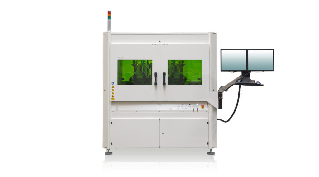
ficonTEC’s series of photonic device testing machines is focused on automated electrical, optical or mixed-signal electro-optical characterization (test-&-qualify) of chips and dies, optoelectronic assembles and integrated devices. This capability includes PIC design validation and device verification.
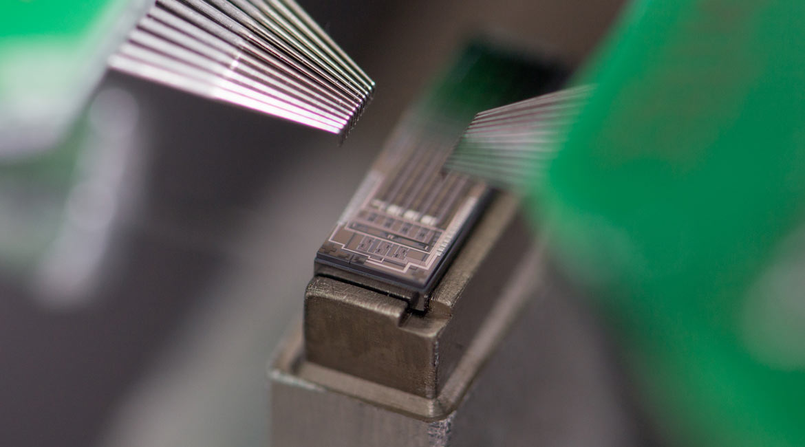
These increasingly complex and miniaturized photonic devices and integrated circuits (PICs) perform advanced optical functions, such as routing, (de)multiplexing switching of optical signals, sensing and data communications. Devices include silicon photonics components, (3D) sensor and lidar assemblies, photonics-enabled medtech devices, MEMS/MOEMS, miniature lasers, HPLDs and fiber pump modules, hybrid assemblies, LED print heads, high-power LEDs, optical communication devices, and many more.
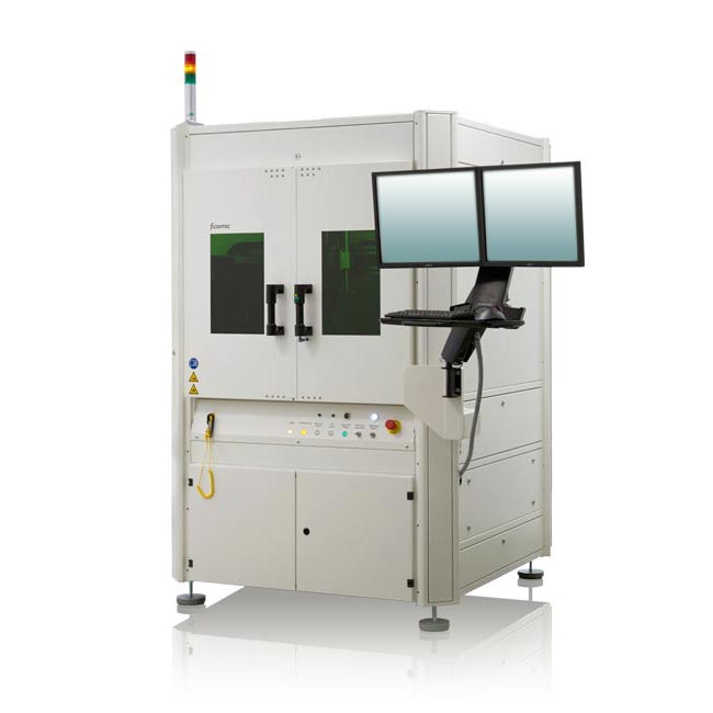
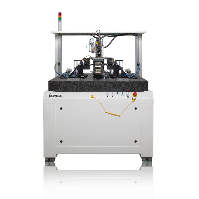
The system checks to see if full optoelectronic functionality meets specifications. The accumulated data is written to an SQL database, providing the user with the necessary statistical analysis and feedback so that, for example, yield can be tracked and improved. The system allows full component tracking and sorting when equipped with a handling system.
The latest integrated device designs, which incorporate both electronic and photonic devices on a hybrid device, provide benefit in terms of functionality, miniaturization, high-volume manufacture and cost/part. Furthermore, the long-term trend towards the uptake of PICs is a key driver for future manufacturing.
However, these high-volume manufactured devices also present a number of challenges during device testing. The long-term requirement will be for ever higher levels of automation and highly parallel, mixed-signal electro-optical testing concepts, both on and off-wafer – a goal to which ficonTEC is already working toward.
Have wafer-level or other specific testing requirements? Get in touch:
Contact usKey Manufacturing Capabilities
-
Testing of singulated devices
-
Wafer-level testing for VCSELs and PICs
-
Testing of fully packaged devices
-
Validation & verification
-
Combined, mixed-signal electro-optical testing
-
Interfacing to test & measurement equipment
-
Fully automated processes
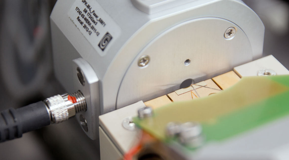
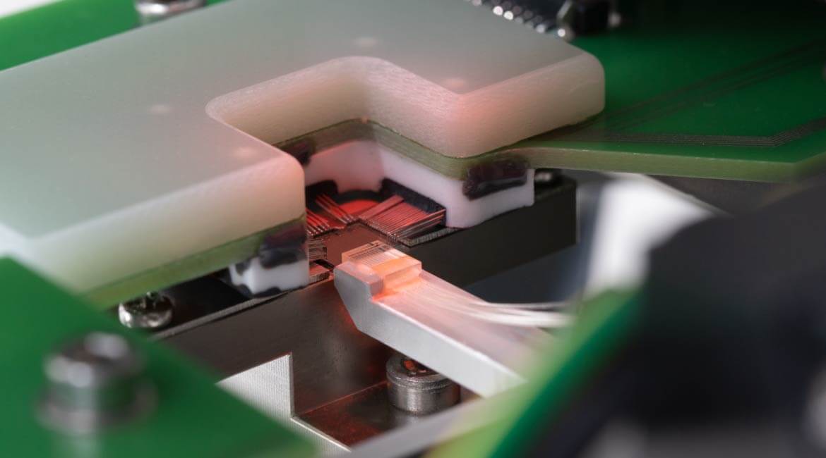
On-wafer passive/active device testing
Fully automated multi-parameter testing
LIV testing and beam characterization
High channel count e/o die test
-
LIV, spectral and far & near-field tests
-
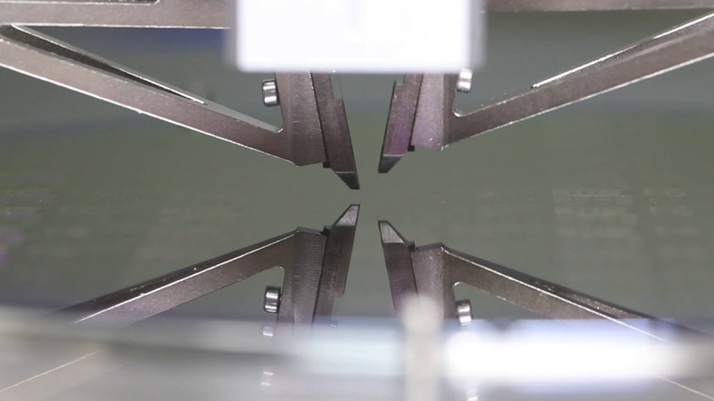
Easy-to-change optical & electrical probe heads
-
Die sorting and component tracking
-
Process parameter tracking
-
OCR for serial number tracking & component traceability
-
Flexible integration of external instrumentation and test protocols
-
Compatible to SQL and other database systems for data traceability
More information
Relevant machine types:
TESTLINE, WAFER TESTLINE
(some test capability available in ASSEMBLYLINE)
Mixed-signal Electro-optical Tester