August 2023
Fully Functional Co-packaged Optical Switch Satisfies Chipmakers’ Need For Speed
ficonTEC has long been well known for its stand-alone photonics assembly & test development systems as well as more recently for the inline capability of its industrial photonic device manufacturing systems. Both these capability suites have also long found favor in the telecom & datacom sector – indeed, ficonTEC R&D systems play an important role in NPI for many global players, and ficonTEC systems additionally make up around 50% of total global manufacturing capacity for the latest commercially available transceivers.
The burgeoning demand for internet bandwidth (not least due to recent advances in access to artificial intelligence services), as well as the vital need to consider the data center device energy budget, has required hyperscale device manufacturers to reassess the e/o architecture. Through the activities of organizations such COBO, this has ultimately led to the embrace of co-packaged optical systems. However, this packaging technology brings with it not only changes in system architecture, but prerequisites new approaches to chip manufacture and packaging. ficonTEC systems are embedded in the thick of these developments. The communications sector is now starting to reap the benefits of the integration of co-packaged silicon photonics into network switches. And where 400G optical transceivers are already being rolled out in data centers, 800G and 1.6T transceiver development is coming to a close.

In fact, having already provided systems for the development and NPI for up to 1.6T devices, ficonTEC is now receiving orders from multiple global players for end-to-end high-volume manufacturing (HVM) solutions. Product launch is scheduled for 2024/2025.
These end-to-end manufacturing solutions are no longer just performing the ‘simple’ lens attach operations of yesteryear. Increasingly they feature high-precision die bonding, high-precision passive or fully active fiber (array) align-&-attach processes and/or multiple-I/O electro-optical chip (die)-level or wafer-level pre-test and end-of-line device test. And this is not exclusively the case for the communications sector – end-to-end capability is increasingly a requirement for many (photonic) device manufacturers across a range of application sectors and is an aspect that ficonTEC can already cater to.
ficonTEC will definitely remain loyal to the development aspect of the integrated photonics eco-system with stand-alone R&D systems, the associated support, and the continued involvement in funded international collaborations. At the same time, integrated photonics manufacturing is ramping up globally, both in terms of volume and in terms of complexity, and ficonTEC is excited to be an essential partner in this vital progression.
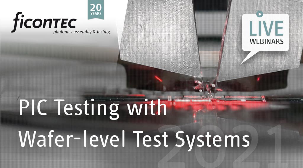
Related Webinar: Wafer-level Test Development Update
The new WaferLine Test product line continues to be rolled out to the first customers worldwide. Starting from the first concept systems delivered in 2019, this first of 3 WLT variants now commonly provides combined electro-optical test for R&D development and low-volume, low-complexity test-&-qualify tasks. However, on the very near-horizon are variants 2 and 3, for batch testing of VCSELs and test-&-qualify of high-complexity integrated devices (think: co-packaging), respectively. Join CEO Torsten Vahrenkamp for an update on what ficonTEC is bringing to the photonics test-&-measurement eco-syste