February 2024
Photonics West 2024 reaffirms ficonTEC’s technical roadmap
SPIE’s Photonics West provides strong evidence for the continued maturity of the integrated photonics sector, with AI driving high demand for CPO devices and for ficonTEC’s advanced automation packaging production solutions.
The 2024 edition of SPIE’s ever successful Photonics West conference and exhibition again staked claim to its prominent role on the global photonics stage by reporting excellent visitor feedback and record overall attendance to the combined event program. The event in general caters to the broader photonics market – laser systems, micro to macro-optical components, cameras and vision systems, materials processing knowhow, test-&-measurement instrumentation as well as tools for the research community. The photonics sector continues to grow at a little over 7 % CAGR, as is evidenced by the latest SPIE market figures.
 For ficonTEC Service GmbH – a global provider of production solutions for high-end optoelectronic and photonic device manufacturing – Photonics West 2024 provides an ideal opportunity to speak with potential and existing customers about developments in advanced automation capabilities for device manufacturing and how these can be beneficially implemented within future production concepts. In addition, long-standing relationships with key global customers in AI-related sectors such as datacom and telecom can be developed in person at the California location.
Finally, the event provides an opportunity to directly observe the role of photonic integrated circuits (PICs, aka silicon photonics) within the broader context of photonics. Strong topics and themes readily visible at Photonics West 2024 included a dramatic increase in entities offering PIC components, diverse component integration/hybridization options and a growing presence of custom manufacturing services. All of this was in particular evidence on the Holland Pavilion, where the collective organizations are represented by the exceptionally well-funded PhotonDelta hub (and to which ficonTEC has close ties).
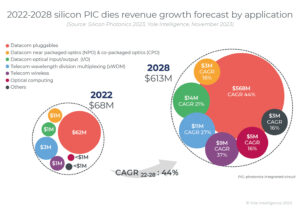 Taken together with the strong upward trend (with CAGR upwards of 40 %) for all aspects of integrated photonics, these signals provide robust reaffirmation of ficonTEC’s current technical roadmap for future development of high-end optical assembly and chip packaging & test production solutions. ficonTEC has, for example, consistently maintained and continues to nurture a very strong production system presence in the communications sector, where advanced manufacturing concepts such as high-level full automation and next-generation chiplet, die-level and wafer-level testing will prove vital in fulfilling even near-term expectations for manufacturing growth requirements. Co-packaged optics (CPO) approaches to device packaging are already being implemented by ficonTEC customers to realize commercially available, high-bandwidth and low-power-consumption CPO components – these are now being utilized to stem the latest surge in demand for compute performance and efficiency as well as communications bandwidth that is in part driven by current developments in AI and the use of associated tools.
ficonTEC can now consolidate on existing priorities for ’24/25, and utilize the renewed understanding to adapt future strategy to keep the company’s offering aligned with future industry needs.
About ficonTEC
 ficonTEC is the recognized market leader for automated assembly and testing machine systems for high-end opto-electronic components and integrated photonic devices. Considerable process capability and dedicated assembly technologies have been accumulated over more than two decades of serving the needs of a broad selection of industry segments – including telecom/datacom/5G, high-power diode laser assembly, IoT-conform sensor devices from bio-med to automotive lidar, micro-optical modules, fiber-optics and more. ficonTEC’s flexible and scalable automation options enable customized assembly and test solutions suitable for early device development, for new product introduction (NPI), and all the way up to high-volume manufacturing (HVM) – regardless of whether for contract manufacturing or for in-house R&D and production.
For more information, visit www.ficontec.com
Related Articles
-

ficonTEC launches next-generation optical circuit switching and the ai era
-

ficonTEC launches DLT-D1, a multi-site die-level tester for double-sided compact 3D CPO optical engines
-

SENKO, BizLink and ficonTEC partner at SEMICON Taiwan 2025 to pioneer advanced ect manufacturing
-

VLC Photonics and ficonTEC Showcase Advanced Automated Die-Level Testing and Assembly at Laser World of Photonics in Munich