June 2021
Combined Electro-optical Wafer-level Testing
One of the remaining frontiers in #photonics_assembly_and_test is volume mixed-signal electro-optical testing. Neither electrical nor optical individually present a major hurdle to developing products and processes (neither singly nor at wafer level), but as soon as the two are mixed, and then also ‘on-wafer’, one is suddenly confronted by a number of issues. Firstly, mixed-signal probe heads need to cater to the different contact scales and device geometries. Secondly, there are for some tests different time scales involved in signal acquisition, thirdly there are scalability issues associated with the concept of parallel testing approaches (think ‘channel density’ & ‘instrumentation’), and fourthly the differing requirements regarding validation vs. verification – the list probably goes on much longer, but that is a good start.
At ficonTEC we started diverting more resources to explore these issues in 2019. Former Business Developer Ignazio Piacentini moved to a full-time role assessing the eco-system requirements for testing VCSELs, PICs and other hybrid devices at wafer-level. He also gave a (albeit) very brief illustration of developments at an online technical meeting organized by EPIC. The current status now (mid-2021) is that this is a fully-fledged resort at ficonTEC, very soon with its own ‘Head of Testing‘.
More recent systems are increasingly mixed-signal e/o test, for example VLC Photonics, based in Valencia in Spain, have recently added a system to their capabilities and are now offering contract test services to their customer base.
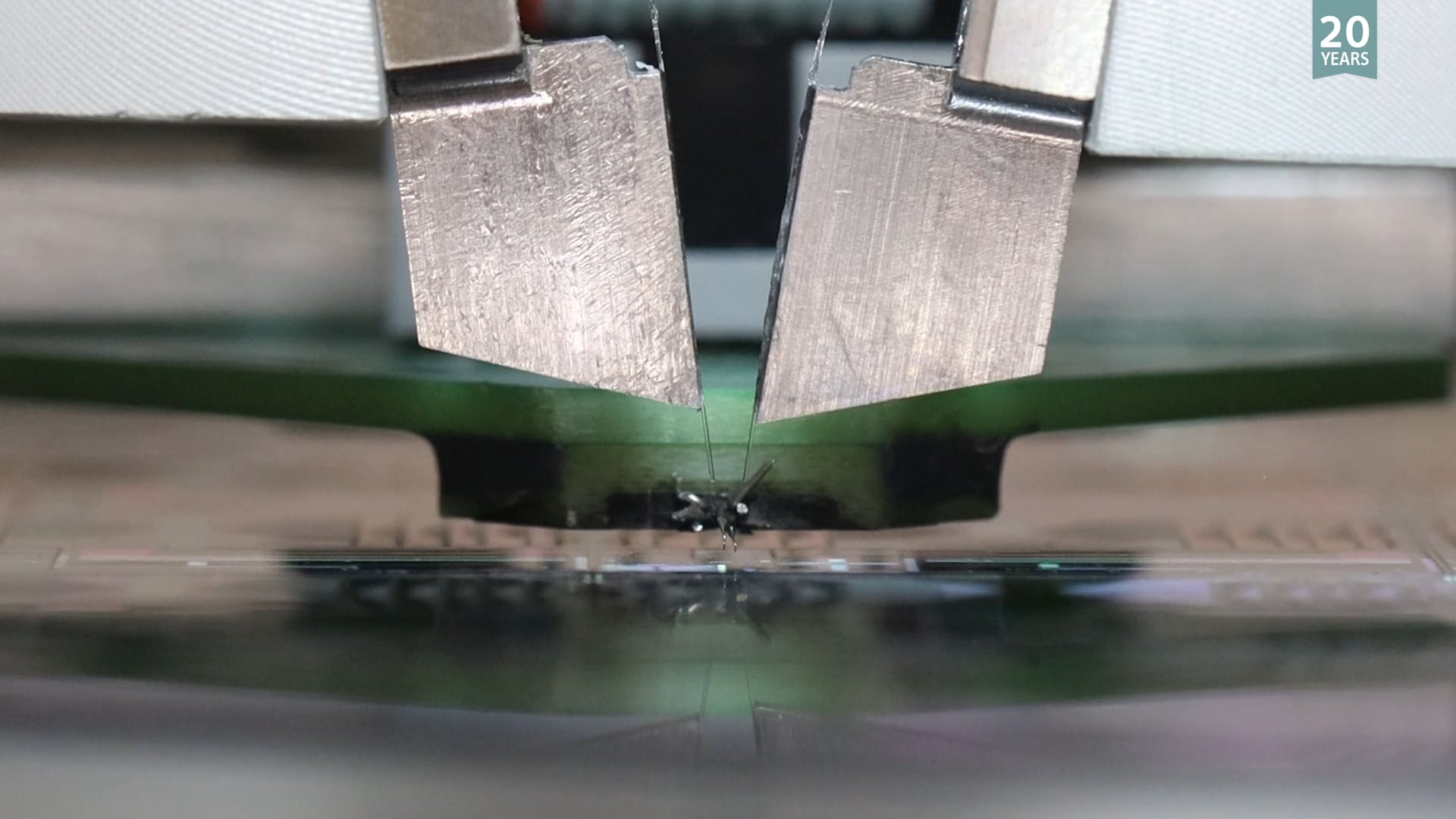
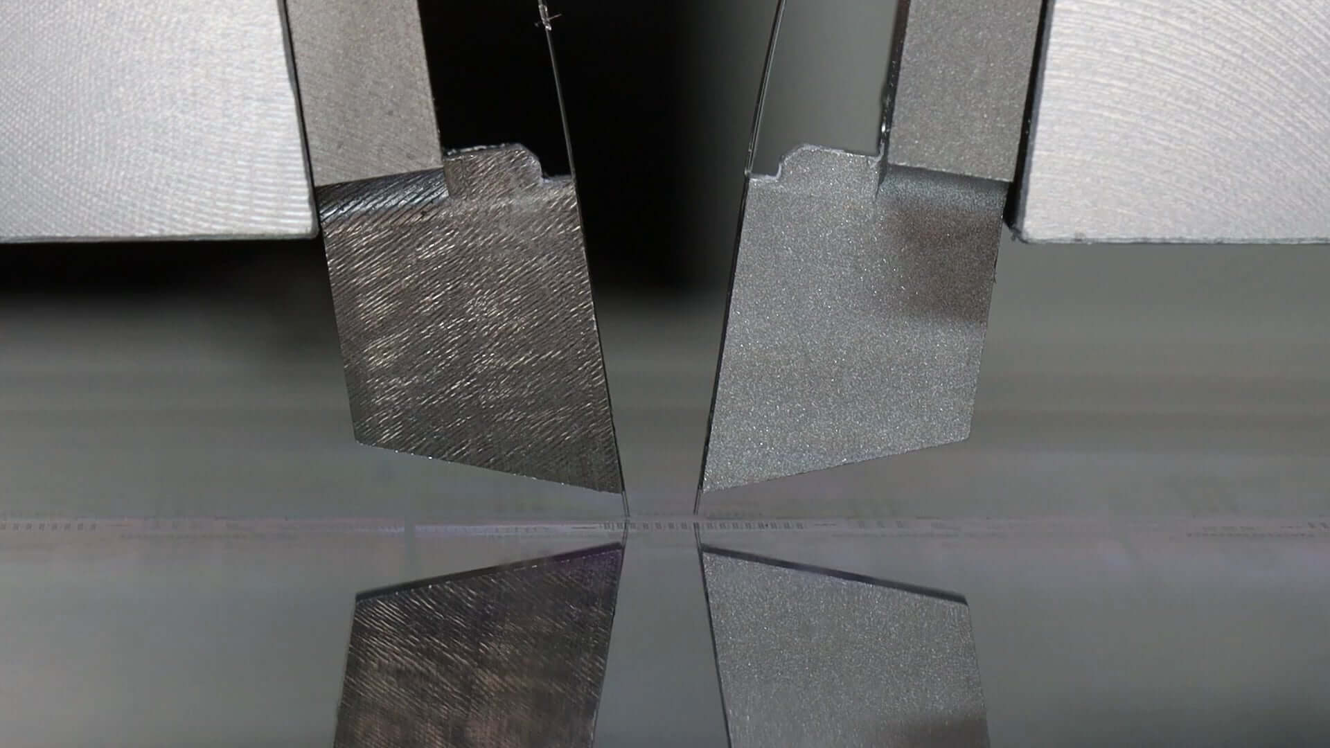
To get a feel for the ‘simple’ wafer-level e/o test systems, this video should provide the viewer with a basic overview of the functionality. And staying with e/o test systems, ficonTEC is already starting to disseminate details of new batch/parallel (x16 – x64 device) testing for VCSELs & PIC channels, timed for release later in 2021. And last but not least, expect solutions for high-complexity devices (multi-mixed-channel) in the mid-term too. To find out more about all of these, you can view our Wafer-level Test Development Update webinar.
If you would like to find out more about the possibilities, please get in touch directly, or reach out to us via our Request Form.
April 14, 2021 – Freely viewable
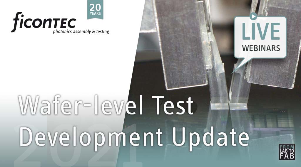
Related Webinar: Wafer-level Test Development Update
The new WaferLine Test product line continues to be rolled out to the first customers worldwide. Starting from the first concept systems delivered in 2019, this first of 3 WLT variants now commonly provides combined electro-optical test for R&D development and low-volume, low-complexity test-&-qualify tasks. However, on the very near-horizon are variants 2 and 3, for batch testing of VCSELs and test-&-qualify of high-complexity integrated devices (think: co-packaging), respectively. Join CEO Torsten Vahrenkamp for an update on what ficonTEC is bringing to the photonics test-&-measurement eco-system.


