

ficonTEC provides device micro-assembly and testing solutions for the photonic device industry. These solutions are realized as cutting-edge, high-precision production systems utilizing advanced automation approaches, regardless of the device material and target application. Our modular system architecture is additionally scalable, so that exploratory, proof-of-process development as well as high-volume manufacturing requirements are addressable – and anything in between.
A globally installed base of over 1000 systems (Q1 2022) is already serving integrated photonics applications in telecom and datacom sectors, for 5G infrastructur, in 3D sensing for smartphone, automotive and aerospace applications, in high-power diode laser assembly, and in many others. ficonTEC is also actively involved in current international initiatives that are designed to reduce time-to-market for integrated photonics technology all within the current transition to high-volume manufacturing processes.
RECENT NEWS

From Innovation to Industrialization: Scaling Optical Interconnects from Test to Assembly
Business News
Integrated Photonics Summit – Watch the recording

Congratulations to Rayhane Ghane on receiving the Best Paper Award
Business News
Best paper award for Rayhane Ghane

ficonTEC launches next-generation optical circuit switching and the ai era
Product News
ficonTEC launches next-generation optical circuit switching and the ai era

ficonTEC launches DLT-D1, a multi-site die-level tester for double-sided compact 3D CPO optical engines
Product News
ficonTEC launches DLT-D1, a multi-site die-level tester for double-sided compact 3D CPO optical engines

SENKO, BizLink and ficonTEC partner at SEMICON Taiwan 2025 to pioneer advanced ect manufacturing
Business News
SENKO, BizLink and ficonTEC partner at SEMICON Taiwan 2025
VLC Photonics and ficonTEC Showcase Advanced Automated Die-Level Testing and Assembly at Laser World of Photonics in Munich
Business News
VLC Photonics and ficonTEC Showcase Advanced Automated Die-Level Testing and Assembly at Laser World of Photonics in…

Discover Brilliant Solutions
The full gamut of process capability captured within a suite of innovative machine systems, all controlled by an advanced software interface
Product Lines – Manufacturing Made Light
Functional machine types designed to provide class-leading flexibility, performance and yield in photonic device production
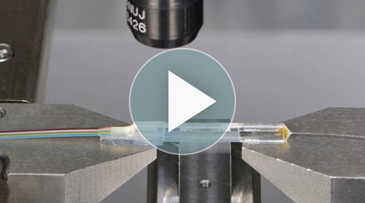
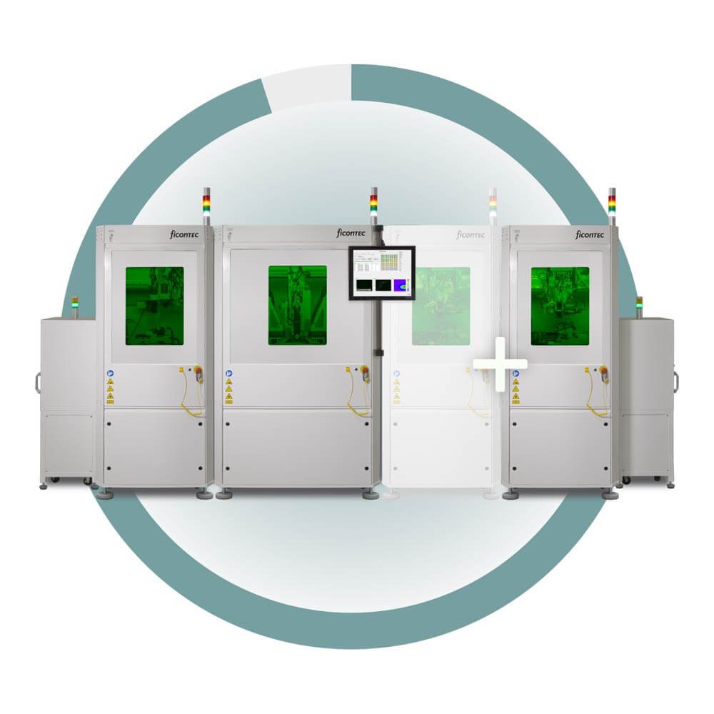
ASSEMBLYLINE
Automated die-level photonic device assembly
- Fully automated passive/active photonic device assembly
- Designed for all optical element, fiber and chip assembly tasks
- Applications in sensors & lidar, HPLDs, co-packaging, PIC assembly
- Next-generation system platform is adaptable ‘From Lab to Fab’
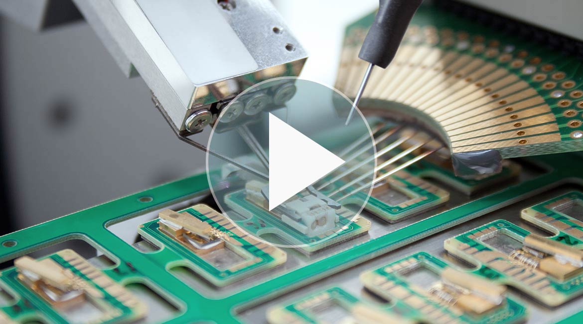
CUSTOMLINE
Flexible, multi-purpose ‘align-&-attach’ platform
- Flexible and highly capable photonic device assembly platform
- For all optical, fiber and die/chip/PIC connection and hybridization tasks
- Designed for collaborative R&D and low-volume/jobshop environments
- For sensors & lidar, co-packaging, SiPh process development and more …
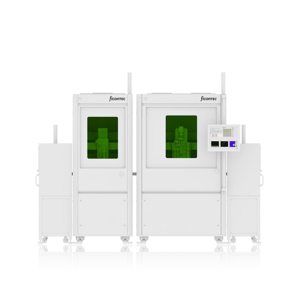
TESTLINE
Die-level photonic device test
- State-of-the-art, mixed-signal electro-optical test
- Fast, high-precision alignment to single/multiple optical I/O ports
- Designed for all optoelectronic devices and PIC material systems
- Next-generation system platform is adaptable ‘From Lab to Fab’
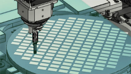
WAFER TESTLINE
Wafer-level photonic device test
- State-of-the-art, mixed-signal electro-optical probing
- Reproducible low-loss alignment to single/multiple optical I/O ports
- Full device referencing/traceability as well as vital wafer yield data
- Fully adaptable to different PIC I/O designs and material systems
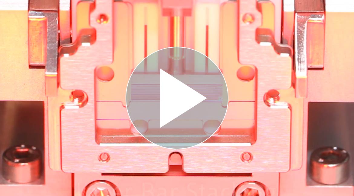
STACKLINE
High-precision device stacking & unstacking
- Precision stacking/unstacking for semiconductor laser diode bars
- Nominal +/- 2 µm, optional +/- 0.5 µm stacking accuracy
- Integrated high-end flowbox and Class 1 laser safety
- Optional optical facet and side wall inspection
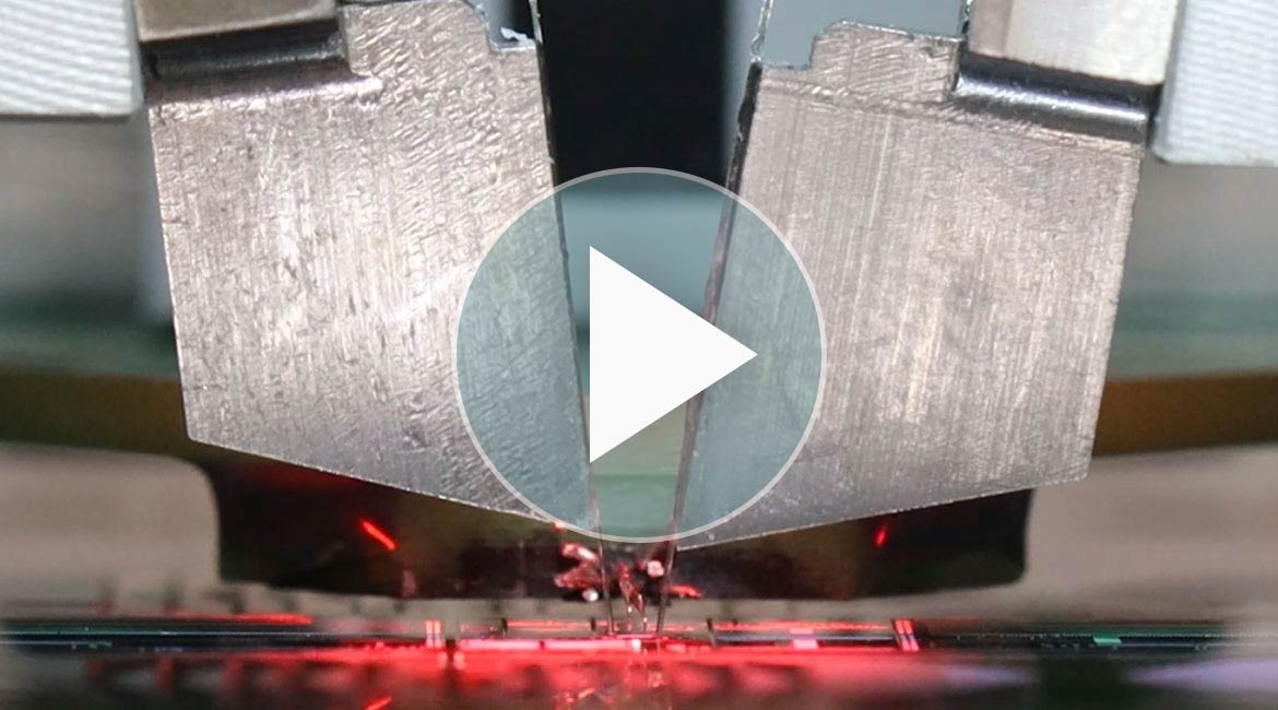
LASER WELD
An automated microwelding station for photonics
- 2 or 3-beam Nd:YAG laser microwelding configurations
- Multi-point or seam welding for ferruled optical components
- Assembled device test-&-qualify, post-weld shift correction
- For terrestrial, aerospace and space satellite applications
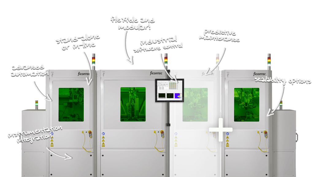
Software Control
Controlled by our flexible process control software, our machines become much more than just the sum of their parts
Learn more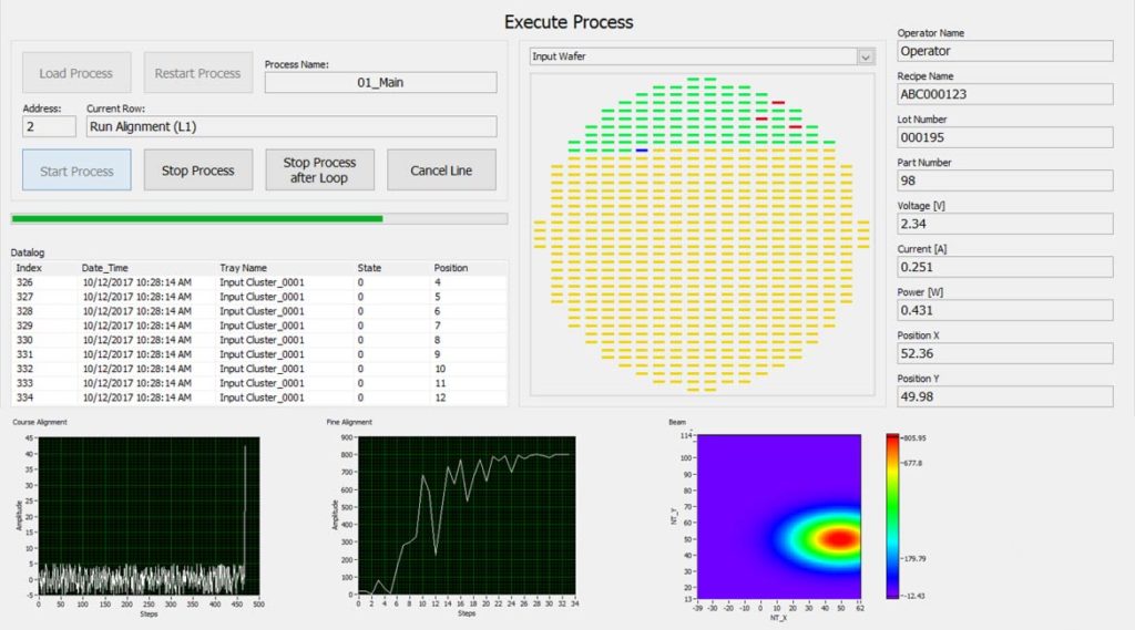
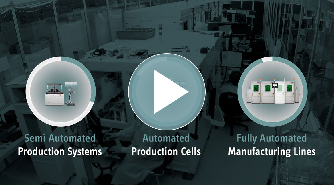
Manufacturing Platforms
Suitable for R&D, process development, complex stand-alone and batch manufacturing, as well as high-volume in-line production
Flexible and scalable options already enable customized assembly and testing solutions suitable for early device development, for new product introduction (NPI), in batch manufacturing, and all the way up to high-volume production facilities involving multiple lines – both for contract manufacturing and for in-house R&D and production.
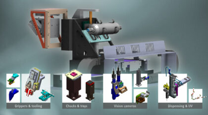
Your Vision Expressed Via Our Process Capabilities
Our production systems embody the customer process, described via a selection of our cutting-edge production capabilities
With over 1000 systems installed worldwide for diverse applications, only ficonTEC offers sufficient breadth and depth of expertise
Assembly and testing remain the highest cost factors in photonic integrated circuit (PIC) production. To address this issue, international collaborations around the globe are actively researching new manufacturing concepts for PIC technology. The goal of these projects is to provide industry with an eco-system that will enable manufacturing to progress from the 1000s to the 100,000s and even millions, from single chip assembly to wafer-level approaches.
ficonTEC has consistently retained involvement in these initiatives in order to stay ahead of industry requirement. Add to this 20 years of development, continually working closely with the customer, and an invaluable modular approach to machine equipment design – all this uniquely places ficonTEC in a position to thoroughly describe your production requirements in terms of industry qualified process capabilities.
Challenge our applications development and process automation teams with your innovative products!
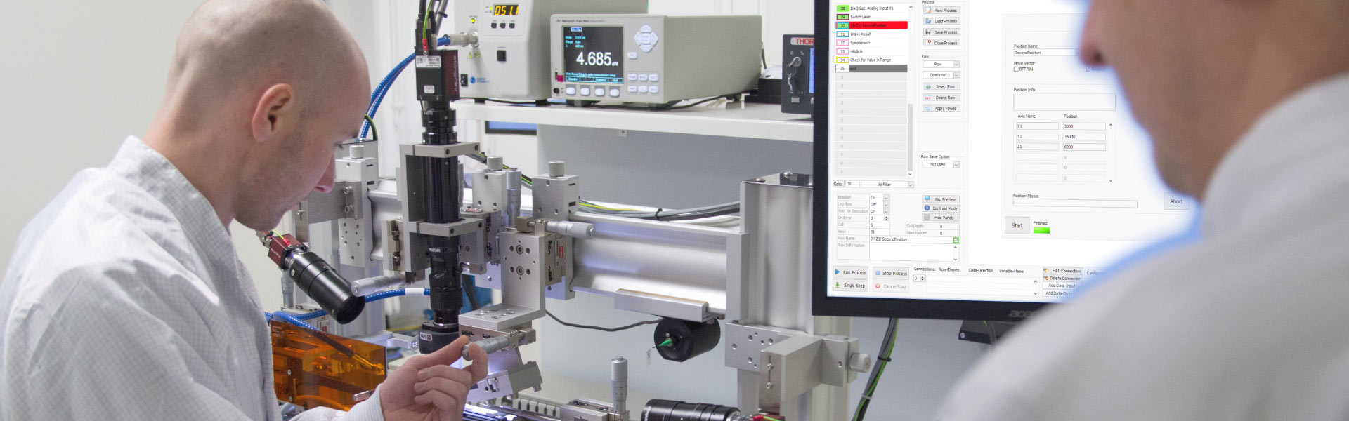
What Is Photonics Assembly And Test?
A brief introduction to the increasingly critical task of photonic device manufacturing
Photonic devices harness light for many important scientific, technical and societal applications. How are these devices assembled?
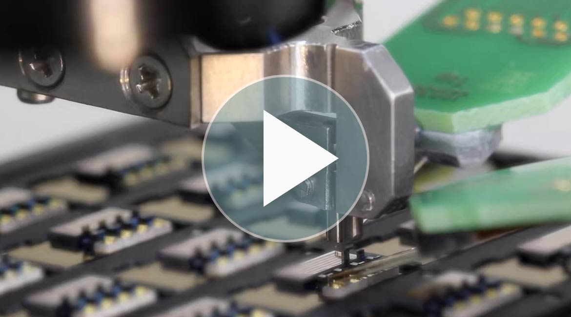
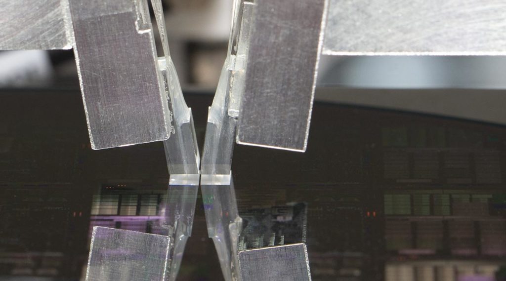
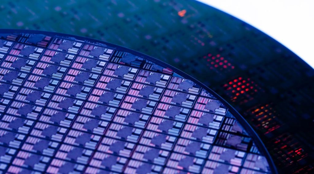
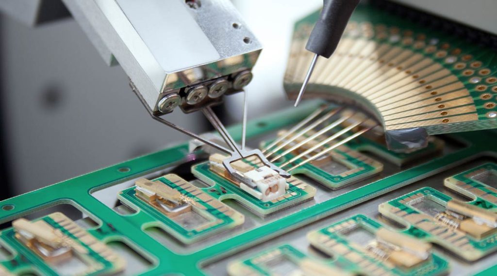
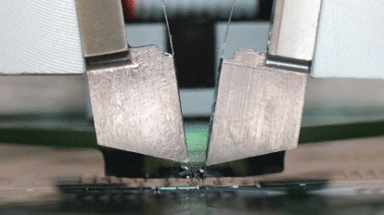
The assembly (align-&-attach) of micro-optical elements, fiber-optic connections and/or optoelectronic chips and components in to finished and qualified photonic devices is what we at ficonTEC categorize as photonics assembly & test. To a degree, this incorporates ‘packaging’ too. Typical devices include telecom/datacom transceivers (TOSA/ROSA/BOSA), infrastructure devices for 5G networks, 3D laser scanners for use in commercial sensing as well as automotive and aerospace (lidar) systems, integrated photonic integrated circuits (PICs), high-power multi-emitter laser assemblies, micro-optical and optofluidic systems, integrated camera modules, and much more.
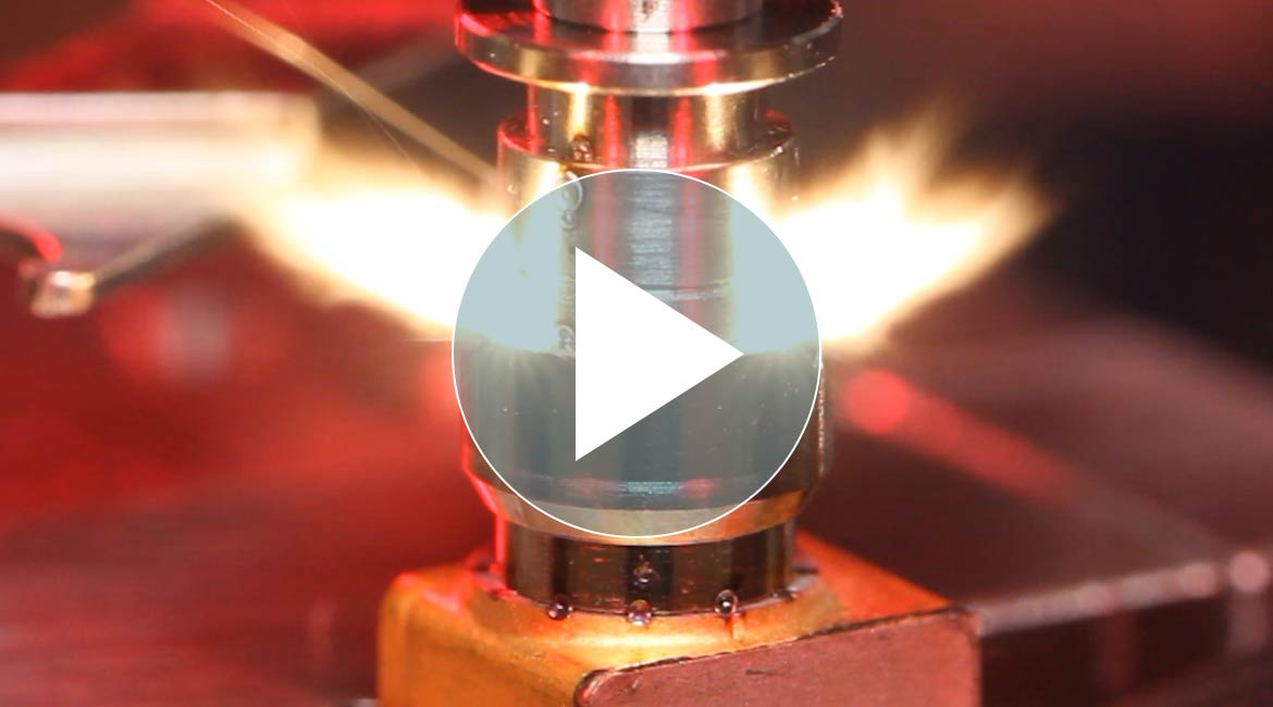
Advanced automation of the assembly process steps requires multi-axis, sub-micron-accuracy (passive/active) component alignment, and subsequent bonding using (UV-) epoxy compounds, thermal-based or laser soldering and/or laser welding. In particular, all manufacturing steps need to be compliant with stringent and often individual requirements for yield, process repeatability and performance reliability, while still enabling minimal process cycle time and minimum downtime.
In-production devices, from simple devices such as laser diode chips and VCSELs, all the way up to the more complex devices noted above, all additionally need testing both at various stages during assembly and at ‘end-of-line’. This often encompasses burn-in, LIV tests, beam and spectral characterization, as well as device design validation and performance verification.
Want to stay up-to-date on developments?
Sign up for our Newsletter and follow ficonTEC on LinkedIN or X (formerly Twitter).
Recent News & Upcoming Events
ficonTEC blog entries, company news and product developments,
and where to find us at events around the globe


ficonTEC INSIDER

Advancing Photonics for Next-Generation Medical Technologies
PhotonMed
Photonics-based medical devices to revolutionize healthcare
Mass manufacturing of transceivers for the terabit/s era – an update
Mass manufacturing
MASSTART – a holistic transformation to assembly and characterization
Mixed-signal electro-optical measurement instrumentation for integrated photonics
Collaboration partnership
Mixed-signal electro-optical measurement instrumentation for integrated photonics-
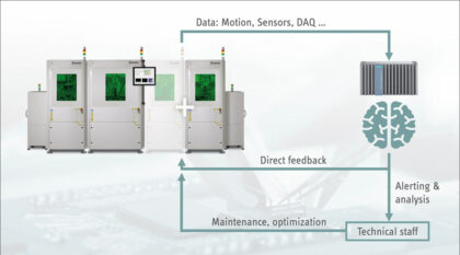
ficonEDGE – Enabling self-help in the Machine
ficonEDGE
Enabling self-help in production systems opens a pathway to lowering total cost of ownership.
Sometimes less is more – A100 base system
A100 base system
Reconfiguration and repurposing made light – addressing the need for flexibility of use.

Fully Functional Co-packaged Optical Switch Satisfies Chipmakers’ Need For Speed
Fully Co-packaged Optical Switch
ficonTEC receives significant orders for end-to-end co-packaged assembly surrounding the push for 1.6T

WE ARE HIRING
Suitable department not listed? Just take a look at our career portal for open positions – Show all jobs
Qualified Employees
We offer interested students of technical disciplines the opportunity to gain an insight into our company through an internship semester or a student research project. You can expect a wide range of tasks in the areas of research and development. Due to the continuously increasing demand for automation for micro-assembly tasks, we are on a growth course and are constantly looking for motivated and qualified employees.
If you are looking for new challenges, why not share your skills with us? We are looking forward to your meaningful application!
